Contents
Overview
This is the sixth article in a series that explores GPIO programming on a Raspberry Pi 3B+. It is an introduction to controlling GPIO peripheral devices by directly interacting with the appropriate registers on the BCM2835 SoC (system on a chip). It is an introduction in that it only covers one of the capabilities, using the basic GPIO capability as described in Section 6 of the BCM2835 ARM Peripherals guide. This excludes BCM2835 support for protocols such as SPI, Pulse Width Modulation, and IC2 which overlay specific protocol capability by utilizing the underlying pins mapped to a given protocol (e.g., GPIO pins 8-11 are associated with the SPI protocol and have behaviors that can be enabled that are specific to that protocol). That said, using the basic pin level functionality covers the same concepts needed to utilize advanced protocol capabilites such as SPI. This article, coupled with the BCM2835 ARM Peripherals guide, should provide enough background to drive devices that are controlled via those capabilities. Of course there are multiple libraries such as the C BCM2835 and WiringPi libraries, the Python pgpio and RPi.GPIO libraries, and the Go go-rpio library that make this much easier. And while these libraries are usually more appropriate for most projects, it can be helpful to understand how the BCM2835 SoC works and how those libraries interact with the BCM2835. This background is also helpful if you find yourself reading library code and/or would like to contribute to these projects, or even write your own library.
This article assumes you already have some familiarity with the BCM2835 and GPIO programming on the Raspberry Pi. If you don’t you may want to consider trying the projects covered in some of my other GPIO articles. The simplist article in the series is Raspberry Pi GPIO in Go and C - Blinking LED. It demonstrates the same capability as this article does, blinking an LED, but it also demonstrates the usage of the WiringPi and the Go go-rpio libraries. It is a good introduction to using GPIO on the Raspberry Pi, but it only covers basic GPIO concepts and how to wire a breadboard to a Raspberry Pi’s GPIO outputs.
The following topics will be covered:
- Prerequisites - describes the hardware and libraries you’ll need for this article.
- An introduction to BCM2835 GPIO Peripherals - provides an overview the BCM2835’s architecture and capabililites.
- Using the BCM2835 board to control an LED via the GPIO pins - provides the details, including code, for controlling an LED using the BCM2835 GPIO registers.
- Summary - summarizes the important concepts covered in this article.
- References - provides a list of references I found helpful, some of which were used in the creation of this article.
Prerequisites
If you don’t have one, you’ll need a Raspberry Pi. I used a Raspberry Pi 3B+ with the ‘stretch’ version of the Raspbian OS. See How to setup a new Raspberry Pi from scratch if you don’t already have a Raspberry Pi and need help setting one up.
Next you’ll need is a breadboard, some jumper wires, a 220 Ohm resistor, and an LED. You should also consider getting a 40 pin female to female with a T-Type adapter to attach the GPIO outputs to the breadboard. You can use only jumper wires, but the adapter will make things easier and will help prevent damage to the GPIO pins on the Raspberry Pi. If you elect not to buy the 40 pin cable with T-Type adapter you’ll need to buy male-to-female jumper wires. Buying all these things separately will cost more than a kit however. Here’s a simple kit that has all of the above. If you expect to follow this series I recommend buying the Sunfounder Raspberry Pi Ultimate Starter Kit.
You’ll need some basic C programming knowledge as well as familiarity with logging on to a Raspberry Pi terminal, or into the desktop GUI that comes with some OS versions. Depending on the approach you take, you may need to connect a keyboard and monitor to the Raspberry Pi. I simply SSH into the Pi. You’ll need familiarity with how to use an editor like Vi or nano. You’ll also need basic familiarity with the Linux command line.
Finally, you’ll need to clone or fork my GPIO repository as it contains underlying library code used to access GPIO capabilities on the BCM2835. As mentioned in other sections, this library code is based on the BCM2835 C library developed by Mike McCauley.
An introduction to the BCM2835 ARM Peripherals
This section provides an overview of the BCM2835 peripherals. It starts with an overview overview of the capabilites of the various types of peripherals. It then moves to an overview of BCM2835 addressing. Understanding addressing is fundamental to understanding the rest of the article. It concludes with a more detailed discussion about how registers are used to access the peripherals and their associated I/O functions.
This is not an exhaustive description of the BCM2835. The only capability that will be covered in any detail, and is the focus of this article, is interacting with the GPIO I/O functions, namely defining the function of a pin and setting and clearing the value of the pin (e.g., setting it to HIGH and LOW), specifically programming BCM2835 GPIO to blink an LED.
There are multiple pin numbering schemes. The Raspberry Pi has physical pin numbers, i.e., the numbers printed on the Pi board. BCM2835 has a numbering scheme called GPIO numbering. It is different than, and incompatible with, the Pi’s physical numbering scheme. Finally some libraries such as the C WiringPi library have their own numbering schemes which are incompatible with the Pi and BCM2835 schemes. This article uses the BCM2835 numbering scheme exclusively. There is a good pin out diagram available that maps between these 3 numbering schemes. Where a pin supports a particular I/O function, as described below, that is also called out on this pin out diagram.
A quick note on terminology… The term “peripherals” is used in the title and in some parts of this article. To me the term peripherals is something of a misnomer. Let me explain. At its most basic the GPIO capability of the BCM2835 is made available through a set of physical pins on the device. Some of these pins provide power and ground needed to drive external devices like LEDs, sensors, and motors. Other pins can be controlled programatically to take input from, or output to, these external devices. At a higher level, subsets of the GPIO pins provide support for complete protocols that implement more sophisticated functions like controlling the speed and direction of a motor and controlling LED displays that display text like those in highway signs. These basic and more sophisticated capabilities are controlled by setting the function of a pin. Input and output are 2 functions that can be set. There are a variety of others that will be covered. Setting the function of a pin describes how the BCM2835 interacts with a device or peripheral. Because of this I prefer to use the term I/O Function. I think that more accurately describes the concept than the term “peripherals” does. To me “peripherals” are the external devices. The first use of the term I/O Functions is the title of the next section.
I/O Functions
The BCM2835 supports a variety of I/O functions. These are the subject of the BCM2835 ARM Peripherals guide. This section will only describe a few of these functions in detail. There are other sources like Wikipedia that can provide information about the others.
The main I/O functions supported by the BCM2835 are:
- GPIO
- SPI
- PWM
- AUX
- BSC
- DMA
- External Mass Media Controller
- Interrupts
- Audio (PCM/I2s Audio)
- System Timer
- UART
As I have direct experience with the first 3 I/O functions, GPIO, SPI, and PWM, this section will focus on these. This will provide enough context in order to get a basic understanding of the kinds of things the BCM2835 is capable of as well as leveraging the information in the Addressing and Registers sections below in order to learn about and use the remaining I/O functions.
GPIO (General Purpose Input/Output)
GPIO stands for General Purpose Input Output. In the BCM2835 ARM Peripherals guide the term GPIO refers to the most general, or basic, level of control of a physical pin. This is what’s used to control the function of a pin, such as setting it as an input or output pin, or more advanced I/O functions such as SPI and PWM. It’s also used to set or get the value of a pin. Values are conceptually referred to as HIGH and LOW, but they are represented by voltage, or lack thereof, passing across the pin. There are other types of settings for pins. One of these settings is used to control whether to detect a state change on the rising or falling edge of a pin’s voltage change. Another setting controls what are called pull-up/pull-down resistors attached to each pin. These resistors are used to explicitly control the value of a pin, 1 or 0, when a pin’s voltage is in an indeterminate state. This tutorial has a reasonably good explanation for why pull-up and pull-down resistors are needed.
The code associated with this article causes and LED to blink. Accomplishing this involves the following steps:
- Set the function of the pin to output, i.e., it’s going to be written to in order to send a signal to the LED.
- Write LOW to the pin to cause the LED to turn on.
- Pause
- Write HIGH to the pin to cause the LED to turn off.
- Repeat steps 2 through 4.
Accomplishing this uses the GPIO I/O functions. More accurately it uses the GPIO registers to set the pin’s function (e.g., output) and to control the behavior of the peripheral, an LED in this case.
SPI (Serial Peripheral Interface)
SPI is used to send data serially to a peripheral that can accept or requires data in parallel. This is helpful because a relatively large set of parallel inputs can be written to using just 3 GPIO pins not including power (VCC) and ground (GND). If SPI wasn’t used, one GPIO pin would be required for each parallel input. This could easily be prohibitive since pins are a limited resource. Let’s see how this works with an example.
The diagram above shows the MAX7219 LED Dot Matrix Display. It’s commonly used to display display arbitrary shapes such as letters, numbers, and smiley faces. It controls an 8x8 matrix of LEDs. Controlling an LED requires 1 pin excluding power or ground. An 8x8 LED matrix has 64 LEDs. This number is well in excess of the 26 or 40 GPIO pins available on a standard Raspberry Pis. As explained below, utilizing SPI requires considerably fewer GPIO pins.
The MAX7219 has the following input pins:
- DIN - this is the serial data input pin.
- CS - This is commonly called a chip select (CS) or chip enable (CE) pin.
- CLK - This pin connects to a clock pin on the Raspberry Pi that synchronizes data transfers between the Raspberry Pi and the MAX7219.
There are 2 more pins that aren’t used to control the MAX7219.
- VCC - This is the power-in pin. It connects to a power source on the Raspberry Pi, usually a 3.3v source.
- GND - This is the ground pin. It connects to a ground pin of the Raspberry Pi.
A minimum of 3 GPIO pins are required to connect from the Raspberry Pi to the MAX7219, specifically to the DIN, CS, and CLK pins. A Raspberry Pi can control all 64 LEDs in a cost (pin-wise) efficient manner using only these three pins. The usual approach is to use the Raspberry Pi pins that can drive the DIN, CS, and CLK pins. These 3 pins are named:
- (SPI)MOSI - This stands for Master Out Slave In. The MOSI pin will be connected to the MAX7219 DIN pin and is used to send a serial data signal to the MAX7219 (or any SPI peripheral).
- (SPI)SCLK - These stand for SPI Clock. This pin will be connected to the MAX7219 CLK pin. It is used as the source of the clock signal used to synchronize the data transfer between the BCM2835 and the MAX7219 (or any SPI peripheral). The data transfer will occur when both the MOSI pin and the SCLK pin are set to HIGH.
- (SPI)CS or (SPI)CE - These stands for Chip Select or Chip Enable. In either case, setting the pin to LOW directs the MAX7219 to accept data as described in the previous bullet.
I reluctantly use the terms “master” and “slave”. However these terms are used in all of the documents I’ve read on SPI. I’ll continue to use them in order to avoid confusion.
The SPI capability on the Raspberry Pi may require as many as 5 GPIO pins. The 2 additional pins are:
- (SPI)MISO - This stands for Master In Slave Out. This pin allows for the MAX7219 (or any SPI peripheral) to send data back to the BCM2835.
- (SPI)CS or (SPI)CE - This is a second chip select/chip enable pin. Having a second CS/CE pin allows the BCM2835 to control 2 SPI peripherals. As stated above, when the CS/CE pin is set to LOW the SPI peripheral will accept data from the BCM2835. So by setting one of the CS/CE pins to HIGH and the other to LOW we can control which slave can receive and send data. The article Using Multiple SPI Slave Devices with the Raspberry Pi provides more information about how the 2 CE/CS pins are used. The following schematic illustrates how this is done:
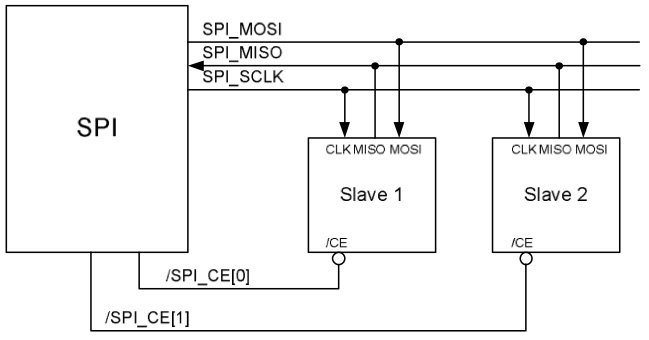
The primary SPI interface on the BCM2835, SPI0, is implemented on GPIO pins 7-11. Pins 7 & 8 are the 2 CE/CS pins available on the BCM2835. Pin 9 is MISO, 10 is MOSI, and 11 is the clock (SPICLK/SCLK). The BCM2835 has 2 auxilary SPI interfaces, SPI1 (AKA AUX_SPI0) and SPI2 (AKA AUX_SPI1). From the BCM2835 ARM Peripherals Guide, SPI1 is available on pins 16-21 and SPI2 on pins 35-39. These auxilary interfaces are available via the AUX I/O function.
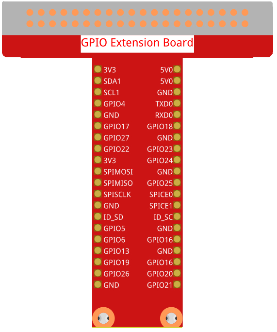
The following diagram shows a GPIO extension board frequently used to connect the BCM2835 GPIO pins to a breadboard. The pins are labeled with there GPIO pin numbers or the I/O function (e.g., SPI) they support Note the SPI pins are labeled on the board using the same terms as above:
In addition to the MAX7219, SPI can be used to control a variety of peripherals to display images, take input from touchscreens, and interact with various sensors. Wikipedia has a good article describing SPI in more detail.
My article titled Raspberry Pi GPIO - Using SPI to display arbitrary patterns on a MAX7219 Dot Matrix Display Module provides detailed coverage of the SPI I/O function and how to program it. Similar to this article, it also includes detailed coverage of how to directly program the BCM2835 using the associated registers on the BCM2835, but for SPI instead of general GPIO I/O functionality. By reading that article you’ll gain a deeper understanding of how to use the BCM2835 registers to program the I/O functionality supported by the BCM2835.
PWM (Pulse Width Modulation)
PWM is used to convert a digital signal, like that produced by the BCM2835, into a simulated analog signal. It is simulated in the sense that it’s not a true analog signal. It’s still a digital signal but it cycles so fast that, much like a video, it appears to be an analog signal. Many peripherals like electric motors, dimmable LEDs, and color LEDs require an analog signal. As with SPI there are dedicated pins that can be enabled to utilize the PWM I/O function. These are GPIO pins 12, 13, 18, and 19. With these pins the BCM2835 supports something called hardware PWM. The PWM functionality is embedded into the BCM2835. It implements a hardware based clock loop that controls the frequency of the simulated analog signal. It is possible to use other GPIO pins for PWM, this is called software PWM. However, in software PWM the clock loop is written in the code that runs on the Raspberry Pi CPU. Since that CPU is doing many other things it isn’t possible to create a reliable clock signal. This can result in some undesirable side effects such as a flickering LED in place of a dim LED. See my articles Raspberry Pi GPIO in Go and C - RGB LED and Pulse Width Modulation for Dummies for more information about PWM as well as examples of PWM in use.
Addressing
All GPIO I/O functions are accessed via registers. These registers are located at various offsets in the on-board memory. Accessing the registers requires a knowledge of how addressing works on the BCM2835 was well as on the Raspberry Pi. Here’s a diagram from the BCM2835 ARM Peripherals guide, section 1.2.1, showing how memory is mapped from the Pi’s physical address to the BCM2835 addresses.
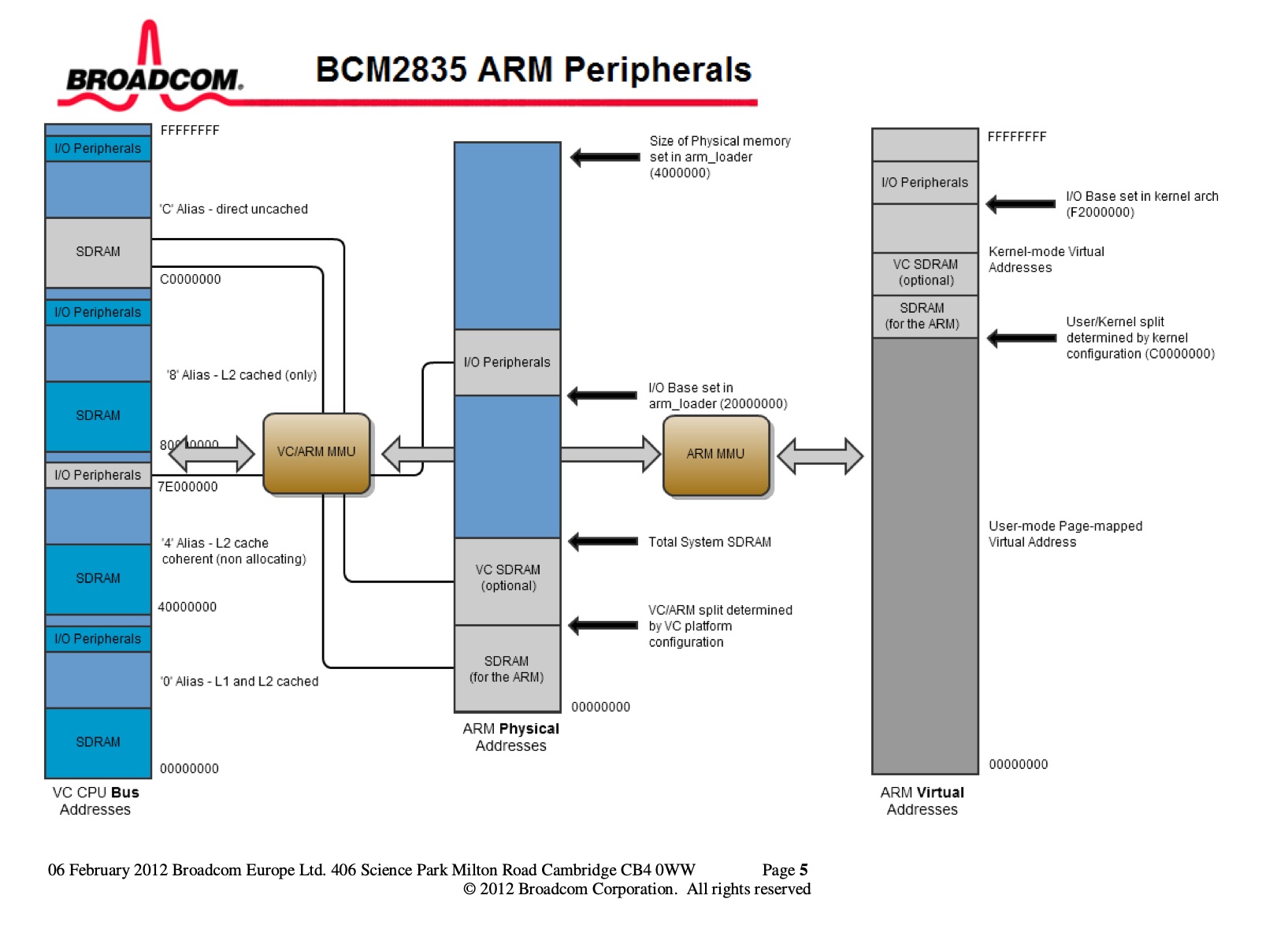
The Raspberry Pi maps the BCM2835 memory to the Pi’s physical address of 0x2000 0000. This is shown in the middle column labeled “ARM Physical Addresses”. The gray shaded area labeled I/0 peripherals is the Pi’s physical memory location of the BCM2835’s peripherals (e.g., GPIO pins). Moving towards the left you’ll see a gold box labeled “VC/ARM MMU”. This is the Memory Management Unit that is responsible for mapping the Pi’s physical memory to the BCM2835 memory. Following the line from the middle column’s “I/O Peripherals” partition, through the VC/ARM MMU, to the far left column titled “VC CPU Bus Addresses” leads to the “I/O Peripherals” partition on the BCM2835’s CPU address bus. It’s address is 0x7E00 0000.
The I/O peripheral addresses can be made available to the application through one of 2 ways. The traditional way is via the /dev/mem device mounted on the file system. Accessing this device requires root privileges. A newer method became available starting with the Raspberry Pi 2. This method accesses the I/O peripheral addresses via /dev/gpio. An advantage of using this method is that it doesn’t require root access. A disadvantage to using this method is that only the GPIO I/O functionality of the BCM2835 can be accessed. This means advanced capabilities like PWM and SPI are not available. Accessing the I/O peripherals using /dev/mem also requires a little more work, namely mapping the physical memory from /dev/mem to the application’s virtual memory. This will be covered in more detail later.
There is third way to interface with GPIO registers. In the case of SPI, there are 2 devices (generally available on many Raspberry Pi models),
/dev/spidev0.0and/dev/spidev0.1viaioctl(). This method won’t be covered in this article.
Registers
As mentioned above, specifying the I/O function of a pin or set of pins is accomplished through registers on the BCM2835. Each I/O function has an associated register set located at an offset within the BCM2835’s I/O peripheral address space. For example, the GPIO register set starts at the CPU bus address 0x7E20 0000. The SPI register set starts at CPU bus address offset 0x7E20 4000. The PWM register set starts at offset 0x7E20 C000. And so on, each I/O function has it’s own set of registers to manage its behavior. That said, they all work on the same principles. Namely, find the offset of the beginning of each I/O function’s register set and then set (or get) the appropriate bits at the appropriate offsets to control the behavior. To make this example more explicit, and to highlight additional details, let’s do a high level walkthrough of how to control a GPIO pin to blink an LED.
As mentioned previously the GPIO register starts at bus address 0x7e2000 0000. Section 6.1 of the BCM2835 ARM Peripherals guide starting on page 90 provides the details about the GPIO registers. To blink an LED we’ll first need to specify the pin’s function, output in this case, and then toggle the value of the LED between HIGH and LOW.
Specify a pin’s function
First the I/O function of the pin needs to be set. A pin’s functionality is defined via one of 8 alternative functions. Encoding each function requires 3 bits, 000 - 111. These bits are contained within what is called a GPIO Function Select Register. Each register is 32 bits long. Therefore each 32 bit register can control 10 pins with 2 bits left over. In order to control all of the GPIO pins there are 6 function select registers. The BCM2835 has the capability to control up to 54 pins, if supported, via function select registers (on the Raspberry Pi 3B+ only 40 pins are available). Supporting 54 pins, with 10 pins/register, requires 6 registers. The first function select register is located at 0x7E20 0000, zero-offset from the start of the GPIO register set. The 6th function select register starts at offset 0x7E20 0014. The 8 alternative functions are:
- Input - represented by bit pattern
000 - Output - represented by bit pattern
001 - and Alternate functions 0 through 5 represented by bit patterns
010through111respectively.
In this example let’s use pin 17 as an output pin. Inspecting the BCM2835 ARM Peripherals guide we see that pin 17 is in function select register 1, AKA GPFSEL1. GPFSEL1 is at offset 0x7E20 0004. Pin 17’s function select offset within the register is at bits 21-23. Recall that the output bit pattern is 001 so we’ll need to put that bit pattern in bits 21-23. In the section on coding below we’ll see how this is actually accomplished.
Set the pin value
This article assumes that pin 17 is attached to the ground terminal of the LED (the cathode). This means that we’ll have to set the pin to LOW in order for current to flow from the power input to the anode through to the LED ground on pin 17 and light the LED. Setting the pin to HIGH will cause the LED to turn off. Switching between LOW and HIGH will cause the LED to blink, which is what we’re looking for.
GPIO pin values are controlled via the GPIO Pin Output Set register. There are 2 GPIO Pin Output Set registers. Pin 17 is in the first register, GPIO Pin Output Set 0, AKA GPSET0, at GPIO register offset 0x7E20 002C. Pin 17 is at bit offset 17 within GPSET0. Setting bit 17 to 1 sets the register to HIGH. GPIO Pin Output Set registers can only set a pin to HIGH, setting a pin to 0 has no effect. But recall we need to set the pin to LOW. Since setting a pin in GPSET0 won’t result in the pin being set to LOW how can we accomplish this? It turns out there is another set of GPIO registers called GPIO Pin Output Clear registers. These are used to set a pin’s value to LOW. Pin 17 is in GPIO Pin Output Clear register 0, AKA GPCLR0, starting at offset 0x7E20 0028. It’s position within the register is also at bit 17. Setting bit 17 to 1 will set the pin to LOW. So we’ll need to left shift a 1 into bit 17 in order to turn on the LED. We’ll use GPSET0 to turn the LED off. As with specifying a pin’s function, how this is accomplished will be covered later in this article. By using the GPCLR0 and GPSET0 registers in turn we can cause the LED to blink.
Other GPIO settings
The GPIO register set can be used to control many other functions of a GPIO pin in addition to selecting the function and setting/clearing a pin’s value. It can also be used to read the value of a pin. As discussed in the I/O functions section above other things that can be managed include specifying how state changes are to be detected (rising/falling edge detection) and how to set the voltage of a pin when it’s in an indeterminate state (pull-up/down resistors). Discussing these other registers is an advanced topic and is beyond the scope of this article.
Setup and Code
This section starts with a program that causes an LED to blink. It’s fairly simple and will show the basic steps needed to program the BCM2835. The next part of this section will cover the BCM2835 programming in more detail. But before all that, here’s how to wire the breadboard to work with the blinking LED example.
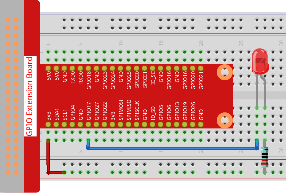
The breadboard should be wired as illustrated in the above diagram. Note that the (bent) long lead of the LED, the anode, is connected to the 3.3 volt power pin via the resister and the cathode, or ground, is connected to GPIO pin 17. If you’re unfamiliar with breadboards and breadboard diagrams this breadboard tutorial should be helpful.
This section will first describe the main program that blinks an LED. After that it goes into detail about how the code that interacts with the BCM2835 works to control the I/O functions.
All code in this article can be found in my gpio repository, in the ledblink directory.
Controlling an LED - main program
The code for the file that contains this code can be found at gpio/ledblink/blinkinglednolib.c.
This first code snippet shows a couple of important things:
- Line 1 gives the command to compile and link the program.
- Line 3 provides the include directive needed to import the BCM2835 functions that directly interact with the BCM2835.
- Line 8 defines the BCM GPIO pin that is used to control the LED. It matches the wiring diagram above.
This snippet declares an interrupt handler to be used to gracefully exit the program. This ensures that the pin, and the LED, are left in a known state. The definition of the interrupt handler will be shown later.
This snippet shows the beginning of the main function.
Line 3 registers the interrupt handler for the SIGINT signal (i.e., ctl-C).
Lines 5-10 initialize the BCM2835 GPIO functionality. Briefly, it finds the GPIO peripherals offset and length within main memory and maps it to /dev/mem so it can be safely accessed within the program. It then sets variables to the offsets of the various capability registers (e.g., GPIO or SPI). If initialization fails the program exits. The bcm_init() function will be described in more detail below.
Line 13 sets LEDPIN to the GPIO output function. This allows the program to write values, HIGH or LOW, to the pin. The bcm_gpio_fsel() function will be described in more detail below.
This snippet implements the primary functionality of the program. Lines 2-10 blink the LED on and off.
Lines 5 and 8 set the value of the LEDPIN by calling bcm_gpio_write() and setting the value of the pin to either LOW to turn the LED on, or HIGH to turn the LED off. LOW turns the LED off because the lead connecting BCM GPIO pin 17 to the LED is connected to the LED’s ground pin. To get current to flow the pin must be set to 0 volts. Likewise, HIGH turns the LED off. bcm_gpio_write() will be described in more detail below.
Lines 6 and 9 cause the program to sleep for 500 milliseconds so the LED can be observed blinking.
As the comment states, line 13 releases the GPIO resources obtained by bcm_init(). This will also set the GPIO system back to a known state. bcm_close() will be described in more detail below.
This snippet defines the interrupt handler function. Lines 3 and 4 first turn the LED off, then release the GPIO resources obtained by bcm_init().
Controlling an LED - interacting with the BCM2835
This section describes how the code interacts with and controls the GPIO peripherals, specifically setting the values of the various registers associated with the I/O functionality of the BCM2835. Setting register values is used to control GPIO peripherals and reading register values allow the current state of the associated GPIO peripherals to be accessed.
The code for the file that contains this code can be found at gpio/ledblink/bcmfuncs.c. The associated header file can be found at gpio/ledblink/bcmfuncs.h.
bcm_init()
The section on Registers mentions that all operations on BCM2835 peripherals are accomplished by manipulating the registers associated for that type of peripheral. The purpose of bcm_init() is to determine the address offsets for all the types of registers, e.g., GPIO, PWM, SPI, etc. so that the their associated peripherals can be controlled.
This snippet shows the beginning of the bcm_init() function.
Line 10 opens the BCM_RPI2_DT_FILENAME. As indicated in the comment, the rb in the fopen() call opens a binary file for reading. BCM_RPI2_DT_FILENAME is defined in the associated bcmfuncs.h header file. It’s value is /proc/device-tree/soc/ranges. As stated in Linux and the Devicetree,
An operating system used the Device Tree to discover the topology of the hardware at runtime, and thereby support a majority of available hardware without hard coded information (assuming drivers were available for all devices).
One of the pieces of information the device tree holds, and is important for our purposes, is the location and length of the I/O Peripherals partition in the BCM2835’s physical address space. Here’s a hex dump of the contents of /proc/device-tree/soc/ranges on a Raspberry Pi 3B+:
pi@pi-node1:/ $ hexdump -C /proc/device-tree/soc/ranges
00000000  7e 00 00 00 3f 00 00 00  01 00 00 00 40 00 00 00  |~...?.......@...|
00000010  40 00 00 00 00 00 10 00                           |@.......|
00000018
We’ll refer back to this in this next code snippet. Per devicetree.org, in v0.4-rc1 of the Devicetree Specification, the soc/ranges property is defined as follows:
The ranges property provides a means of defining a mapping or translation between the address space of the bus (the child address space) and the address space of the bus node’s parent (the parent address space). The format of the value of the ranges property is an arbitrary number of triplets of (child-bus-address, parent-bus-address, length)
In the case of the I/O Peripherals address block, as described in the Addressing section above, the “child-bus-address” refers to the “I/O Peripherals” address block in the “VC CPU Bus Addresses” memory space. The “parent-bus-address” refers to the the “I/O Peripherals” address block in the “ARM Physical Addresses” block. And the “length” refers to the actual length of the “I/O Peripherals” address block. The Raspberry Pi 3B+ has a 32 bit address space so each of the values in the triple are 32 bits or 4 bytes.
This next code snippet finds the parent-bus-address and length of the I/O peripherals block using the data from /proc/device-tree/soc/ranges. Recall that the parent bus address is the second entry in the triplet that also defines the child bus address and length. Lines 1 thru 4 shift the contents of the parent-bus-address, bytes at buf offsets 4 thru 7, into base_address. 3F is shifted into the high order byte of base_address. The remaining buf cells are likewise shifted into base_address from left (most significant) to right (least significant byte). After shifting is complete base_address will be set to 0x3F000000. Looking back at the diagram in the Addressing section above you’ll notice it DOESN’T MATCH the base address of 0x20000000 in the I/O Peripherals address block in ARM Physical Addresses. This is because the diagram in the Addressing section is for the Raspberry Pi 1. This offset is different in the Raspberry Pi models 2 & 3. And it’s different yet again in the Raspberry Pi 4 model.
Moving on, in a similar manner to base_address, lines 6 thru 9 get the length by shifting from buf offsets 8 thru 11 into peri-size. For the Raspberry Pi 3B+, 0x01000000 is the expected length of the address block.
This next code snippet completes obtaining the addressing information from /proc/device-tree/soc/ranges. Specifically it validates that the “child-bus-address” and “parent-bus-address” have the expected values. Recall that the “child-bus-address” is the first value in the addresses/length triplet, buf offsets 0 thru 3. Lines 1 thru 6 do the following:
- Lines 1 thru 4 verify that the first 4 bytes of
buf, the child-bus-address, is0x7E000000as defined by the “I/O Peripherals” address block in the “VC CPU Bus Addresses” memory space. - Line 5 verifies that the parent-bus-address,
base_address, matches one of the expected base addresses for Raspberry Pi models 1 thru 4.
Lines 7 and 8 then set the base address and length of the I/O Peripherals address block to the variables that will be used in the rest of the program. The important thing about this line is that it casts the source variables to the types expected by the target variables.
This next snippet maps the BCM2835’s “I/O Peripherals” address block in the “ARM Physical Addresses” memory space from /dev/mem so that it can be safely used in the program.
Line 1 first checks to see if the user running the program is running as root (either root user or sudo). If not, the /dev/mem device can’t be used. /dev/mem provides unrestricted access to the CPU’s memory. As this is obviously a dangerous thing to do its use is restricted to root. As you may recall from the Addressing section, there is an alternative to /dev/mem, /dev/gpio. This will be shown later in this section.
Line 4 opens /dev/mem in preparation to the mapping operation.
Line 13 assigns the bcm_peripherals variable to the offset and length, bcm_peripherals_base and bcm-peripherals_size, of the I/O Peripherals address block. This mapping effectively restricts the program’s access to the I/O Peripherals address block of physical memory.
This next code snippet calculates the offsets for the various types of registers (e.g., GPIO, PWM, SPI, etc). Each offset is relative to the value of bcm_peripherals which was the result of a mapmem() operation in the previous snippet. So to get the address of a register set like the GPIO register set we would add BCM_GPIO_BASE to the bcm_peripherals base address. But you may have noticed the code divides these offsets by 4 prior to adding them to bcm_peripherals. These offsets, e.g., BCM_GPIO_BASE, which are specified as integers, point to specific byte addresses, i.e., at 8 bit boundaries. bcm_peripherals is specified as a uint32_t*, a pointer. You can’t just naively add an integer to a pointer. You may recall that pointer arithmetic operates on a pointer variable based on the size of the type of the associated variable. For unint32_t's their size is 32 bits or 4 bytes. Adding 1 to a uint32_t pointer will result in that pointer pointing to the next uint32_t, which starts 4 bytes from the current position. Naively adding offsets like BCM_GPIO_BASE to bcm_peripherals will result in bcm_peripherals pointing to a position in memory that is 4 uint32_ts past the current position, not 1 uint32_t past the current position which is what we want. Which is why each register type offset like BCM_GPIO_BASE is divided by 4 prior to adding it to bcm_peripherals.
If you’re new to C you may not be aware that pointer arithmetic is inherently dangerous. It can be hard to know exactly what a pointer will reference as a result of pointer arithmetic. The pointer could be an unexpected type or have an unexpected value. This can lead to unexpected behavior which can be very difficult to debug. In some cases, for example performing division, pointing to an unexpected place that contains the value zero will lead to the program abruptly ending (with a segmentation fault). This is good, this way you know something is wrong and you even know where it went wrong. A pointer may even point outside the program’s address space the program which may lead to system crashes. In our case however the register locations and associated types are very well known and using pointers is relatively safe. That is, as long as we perform pointer arithmetic correctly…
bcm_fsel()
bcm_fsel is responsible for setting the I/O function associated for a given pin. There are a total of 8 functions available. One defines that the associated pin is to be set as an input pin meaning that it will be read from. Another function defines the associated pin as an output pin meaning the pin will be written to. The remaining 6 are referred to as “alternate functions” and are given names like “alternate function 0”. The I/O function that is assigned for the various alternate functions is different for the various GPIO pins. For example, setting BCM GPIO pin 17 to alternate function 4 defines its I/O function to be SPI. It actually defines the pin to be a specific subset of SPI functionality called chip enable or chip select, but that is a topic for a later article. Recall that in main() above, the function is being set to BCM_GPIO_FSEL_OUTP which defines pin to be an output pin.
There’s quite a bit going on in this function even though it is quite short.
Line 1 defines the function as taking two parameters, pin and mode. It is fairly obvious that pin the pin whose function is to be assigned. mode is the I/O function to associate with pin. mode is actually a bit pattern to be assigned to a particular register offset. The bit pattern assignments are defined in the The BCM2835 I/O Peripherals datasheet in section 6, GPIO. The patterns are defined as follows:
000 = GPIO Pin X is an input
001 = GPIO Pin X is an output
100 = GPIO Pin X takes alternate function 0
101 = GPIO Pin X takes alternate function 1
110 = GPIO Pin X takes alternate function 2
111 = GPIO Pin X takes alternate function 3
011 = GPIO Pin X takes alternate function 4
010 = GPIO Pin X takes alternate function 5
There is some additional background needed to understand the rest of the function. First, The BCM2835 I/O Peripherals datasheet, section 6, shows that a total of 54 GPIO pins are addressable via the function select registers (GPFSEL0-GPFSEL5). Each function select register is 32 bits long. Since each of the function select patterns above is 3 bits long each function select register can specify the I/O function for 10 pins with 2 bits left over. Ten pins per register and a total of 54 pins explains why there are 6 function select registers numbered 0 thru 5. The math that follows is derived from this information.
Line 3 defines the register offset, paddr, of the bits that will be set according to mode. BCM_GPFSEL0 is the base offset, in bytes, of the function select registers. Here’s an explanation of the arithmetic performed in this line.
- Notice that pointer arithmetic is being performed. Recall that the result of pointer arithmetic is based on the type of the target variable (see the bcm_init() section above). Since
uint32_t's are 4 bytes longBCM_GPFSEL0needs to be divided by 4 for the calculation to come out correctly. Hence... paddr = bcm_gpio + BCM_GPFSEL0/4 .... - Also recall that each register holds the function select information for 10 pins. For a given pin we need to determine which function select register, GPFSEL0 thru GPFSEL5, specifies the I/O function for a given pin. In C, the result of integer division that results in a fraction will be rounded down. So if we divide the pin number by 10,
(pin/10), we’ll get the offset to the correct function select register. So pin 9 will result in9/10which equals 0, meaning pin 9’s function select location is in GPFSEL0. Likewise, pin 17’s,17/10 = 1, function select register is GPFSEL1. And so on.
Taken together, the equation paddr = bcm_gpio + BCM_GPFSEL0/4 + (pin/10) results in the function select register offset appropriate for a given pin. For pin 17 this will result in paddr logically pointing to GPFSEL1 at address 0x7E20 0004, 7E being the bus address, 20004 being the offset of the GPIO registers plus the offset of GPFSEL1, 4, from the beginning of the GPIO register set. I say logically because bcm_gpio is an offset from an address returned as the result of a mmap() operation. mmap() returns a pointer into the process’s virtual memory whereas 0x7E20 0004 is an address in the BCM2835’s VC CPU Bus Addresses space.
Line 4 calculates the location within the function select register for given pin’s function select value. Since we’ll use bit shifting to set the pin’s function select value this location becomes the number of bits to SHIFT the pin’s function select value as provided in the mode parameter. Building the calculation up we first need to find the pin’s logical location, that is, which 3 bit cell within the function select register (recall that each function select value is 3 bits long). The calculation for this is given by shift = (pin % 10) .... For pin 17 (pin % 17) = 7. So pin 17’s 3 bit cell is located at the 7th 3-bit offset. Next we have to find the actual bit offset within the register. Since each function select value is 3 bits long each pin’s boundary is a multiple of 3, hence the complete calculation of shift = (pin % 10) * 3. For pin 17 this results in (17%10)*3 which equals 7*3 which results in an absolute bit offset of 21. Consulting the BCM2835 I/O Peripherals datasheet, section 6, on page 92, we can confirm that pin 17’s offset within the GPFSEL0 register is in bit positions 21 thru 23.
Now let’s look at line 5. When setting a subset of bits to a given value we want to preserve the values of the surrounding bits. A mask is used to accomplish this. The mask contains a bit(s) that is in the position of the bit in the target value that we want to change. For example, in the bit pattern 0101 1111, if we want to set bit 6’s value from 1 to 0 we only need to define a bit sequence with 1 bit set. To create the most general solution we would just set the least significant bit(s). Since we only need a single bit set we would define the mask as hex number 0x1, which specifies the bit pattern 0000 0001. Next we need to shift this bit pattern as required so that the 1 bit is moved to the correct position. In our example, since we want to change bit 6, we would left shift the mask pattern 6 bits to the left, e.g., newMask = 0000 0001 << 6. This results in newMask equaling 0100 00000, which is puts the 1 bit in position 6 as we desire. It’s possible that we could have defined the mask as 0100 0000 outright, but this would not result in a general solution that would work for any mask needed to set a bit(s) in an arbitrary bit position, such as bits 21-23.
As given in bcmfuncs.h the value of BCM_GPIO_FSEL_MASK is 0x7 or 0000 0111, this is because each GPIO function select pattern is 3 bits long. So this is a useful bit pattern for masking 3 bit sequences. If we shift this pattern by the SHIFT of 21 as calculated in line 4 above we’ll get a 32 bit pattern that looks like this, 0000 0000 1110 0000 0000 0000 0000 0000. The mask is now in bit locations 21-23, which is the location of pin 17’s function select pattern in the GPFSEL1 function select register.
In summary, line 5 creates the mask needed to set the 3 bit function select pattern as specified in the mode parameter on the provided pin parameter.
Line 6 creates the new 3 bit value that will be placed into the GPFSEL1 register. Recall that GPFSEL1 is a 32 bit register. To use a 3 bit value such as mode to set a 3 bit sequence at an arbitrary position, e.g., bits 21-23, we create a value mask that sets the bits in the desired position to the desired value. As with the mask above, the most general solution specifies that those bits be set starting in the least significant position. Let’s say in our example we want pin 17 to be set to alternate function 1. Looking at the bit patterns above we can see that the 3 bit value for alternate function 1 is 101. The mode parameter will contain this value. To set pin 17 to alternate function 1 we need to shift mode's bit pattern of 0000 0101 21 bits to the left. As with line 5, line 6 does this in a general way, value = mode << shift. Given our value of mode and the calculated value of shift we get the 32 bit value of 0000 0000 1010 0000 0000 0000 0000 0000.
So we now have the 4 variables needed to calculate the new value of the GPFSEL1 register, paddr, mode, mask, and value.
Line 7 calls the function bcm_peri_set_bits() to complete this operation. This operation is done in a separate function since there are other register values that require setting as we will see later.
bcm_peri_set_bits()
bcm_peri_set_bits() is the function that sets a 32 bit sequence, v, to a new value, value, at position paddr, using a mask as discussed above. As with bcm_fsel(), this function does quite a bit in just a few lines of code.
Line 3 uses bcm_peri_read() to read the 32 bit value v located at paddr. More on this later.
Line 4 sets the v to its new value. Recall that when a mask is used a subset of bits can be set while leaving the remaining bits unchanged. Line 4 does this in 3 steps. First it does a bitwise-AND operation, &, between the current value v with the complement of mask. Taking the example in the previous section for BCM_GPIO_FSEL_MASK, it’s bit value, for brevity just bit positions 16 and 23, is reversed from ... 1110 0000 ... to ... 0001 1111 .... When the bitwise-AND occurs between the the complemented mask and v as in (v & ~mask), only the bits 21-23 of the original value v are modified and bits 21-23 are reset to 0s. The remaining bits are unchanged. If bits 16-23 of v were originally set to ... 0100 1010 ..., the new value of bits 16-23 will now look like ... 0000 1010 .... In our example for pin 17 its function select bits have been reset to zeros. Note the bits in positions 16 thru 20 are unchanged.
The next operation, (value & mask) only retains the bits values at positions 21-23 of the new value, value, setting the remaining bits to 0. Bits 16-23 of value are ... 1010 0000 ... which specifies pin 17 is is to be set to alternate function 1. The result of the operation ... 1010 0000 ... & ... 1110 0000 ... is ... 1010 0000 ..., which is expected. The operation is specified as (value & mask) because we can’t say ahead of time that only bits 21-23 are to be reset to value. Both value and mask could have bits set at other positions.
Putting this all together, the third and final step, (v & ~mask) | (value & mask) will OR the 2 results, ... 0000 1010 ... | ... 1010 0000 ... which results in v being reset to ... 1010 1010 .... Remember that only bits 21-23 were changed. This is shown here by bits 16-20 retaining their previous values. Likewise, the other bits ov v will remain unchanged.
Line 5 the sets the 32 bits at paddr to v via bcm_peri_write(). More on this later as well.
bcm_peri_read()
bcm_peri_read() will read the 32 bits starting at paddr and return them to the caller as a 32 bit value. Unlike bcm_fsel() and bcm_peri_set_bits() this function is quite simple.
Lines 4 & 6 synchronize access to memory so that the read can’t be interrupted.
Line 5 simply sets the return value, ret, to the contents located at paddr.
bcm_peri_write()
bcm_peri_write() will write the 32 bits starting at paddr to the value contained in value. Like bcm_peri_read() this function is quite simple.
Lines 3 and 5 synchronize access (lock) to the 32 bits starting at paddr.
Line 4 sets the 32 bits located at paddr to value.
bcm_gpio_write()
bcm_gpio_write() writes the 32 bit value to the specified pin. It uses 2 helper functions, bcm_gpio_set() and bcm_gpio_clr(). The parameter on is used to specify if the value for pin should be set or cleared. There are a set of 4 GPIO registers, GPSET0 and GPSET1, and GPCLR0 and GPCLR1, which specify if the value of a pin is HIGH or LOW. HIGH corresponds to GPSETn. LOW corresponds to GPCLRn. When the value of on is 1 the GPSETn register associated with the value of pin is set to 1. If on is set to 0 then the GPCLRn register associated with the value of pin is set to 1. GPSETn’s values are only used when a pin’s I/O function is set to OUTPUT. GPCLRn’s values are likewise only used when a pin’s I/O function is set to OUTPUT. Values of 0 in these registers are ignored. Recall that the BCM2835 allows GPIO functions to be specified for 54 pins (vs. the expected 40). Since each pin requires 1 bit to specify whether it’s to be set or cleared a total of 54 bits is required. This explains why two 32 bit registers are needed for set and clear.
The use of these registers is further described in section 6, page 95, of the BCM2835 I/O Peripherals datasheet.
bcm_gpio_set() and bcm_gpio_clr()
bcm_gpio_set() and bcm_gpio_clr() are twins in terms of their functionality. They only differ in which registers they operate on. *set() operates on the GPSETn registers and *clr() operates on the GPCLRn registers. They are responsible for setting the appropriate bit offset in the appropriate register for the provided pin argument. This section will only describe bcm_gpio_set(). With the exception of the register set operated on their implementations are identical. In fact, with the addition of another parameter to specify the starting offset they could be collapsed into a single function.
In bcm_gpio_set() line 3 calculates the address, paddr, of the target register. bcm_gpio is the starting offset of the GPIO registers. BCM_GPSET0 is the starting offset of the set and clear registers. Recall from the discussion in the bcm_init() section above that pointer arithmetic is used to determine the memory offset to use for a given operation. This is why BCM_GPSET0 is divided by 4 in this operation. pin/32 is used to calculate which of the GP*n registers is to be used for the given pin. Recall that integer division always rounds down. So the result of pin 17/32 is 0 which specifies that the first GP*n register will be used. This is consistent with the BCM2835 ARM Peripherals guide. And 0 is correct in the calculation of the paddr because of the use of integer arithmetic.
Line 4 calculates how large of a shift is needed to set the proper bit associated with pin in the GP*n register. Taking our example of pin 17, 17%32 is 17, which corresponds to bit 17 in GPSET0. Again, per the BCM2835 ARM Peripherals guide, this is the correct offset within the correct register.
Line 5 then uses bcm_peri_write() to shift 1, shift bits to the left, in order to write to the correct offset in the correct register. From the calculation on line 4, 1 is shifted 17 bits to the left.
bcm_close()
bcm_close deallocates all resources and resets all GPIO offsets to their original values, MAP_FAILED in this case. With regard to MAP_FAILED, this value prevents any more operations on the BCM2835 peripheral registers.
Line 3 releases the memory reserved by the mapmem() operation in bcm_init().
Lines 4-14 reset all the register offsets to their default settings.
Summary
This article has provided a detailed look at how to interact directly with the BCM2835’s peripherals registers, without using a 3rd party library, to make an LED blink. It first provided an overview of the BCM2835’s ARM peripherals main concepts including the types of I/O functions that operate on external devices/peripherals, how the BCM2835 addressing works as a prerequiste for describing how to interact with the BCM2835 registers to control external devices (like an LED). It then described the lab setup needed to control an LED. Next it presented the code, along with explanations of what the code is doing, used by the main program. It finished up presenting the code, with explanations, that interacts directly with the BCM2835’s registers that are associated with various types of peripherals.
At this point you should have a good understanding of how to directly program the BCM2835 to control a variety of peripheral types using the various I/O functions supported by the BCM2835. While the low-level details for a specific I/O function, e.g., SPI, may differ, the mechanics for programming the BCM2835 are the same.
Keep an eye out for my upcoming article titled “Raspberry Pi GPIO - Using SPI to display alphanumeric characters on a MAX7219 Dot Matrix Display Module” which, among other things, will demonstrate how to control a dot matrix LED display using only low-level access to the BCM2835 registers. It makes a nice companion to this article as it will introduce a new set of peripheral registers used to program the SPI I/O function.
Comments and questions about this article are welcome.
References
- The Sunfounder Blinking LED project is the source of the breadboard diagram. It was also the inspiration for this series on Raspberry Pi GPIO programming. See my Blinking LED project for more details.
- Raspberry Pi GPIO Pinout diagram including the physical board pin numbers, the BCM/GPIO pin numbers, and the WiringPi pin numbers.
- The gpio repository containing the code for this and other articles
- How to setup a new Raspberry Pi from scratch
- How to use a breadboard
- GPIO programming on a Raspberry Pi 3B+ contains a list of my articles about GPIO programming on the Raspberry Pi
- The BCM2835 Peripherals guide.
- The C BCM2835 library by Mike McCauley
- The C WiringPi library and associated GitHub repository
- The Python pgpio library
- The Python RPi.GPIO library
- The Go go-rpio
- Linux and the Devicetree describes what a Linux device tree is and how it is used.
- Using Multiple SPI Slave Devices with the Raspberry Pi provides more information about how to use multiple slave devices.