Contents
Overview
This is the fifth article in a series that explores GPIO programming on a Raspberry Pi 3B+. It is a supplement to the Sunfounder 7-Segment Display project. You can find the full series here. The code for the series can be found on github.
Like the Sunfounder RGB LED project, there are some complicated aspects to this project that aren’t well covered in the Sunfounder project documentation. The purpose of this article is to fill those gaps, specifically:
- What is a “shift register” (the 74HC595 chip)?
- What are the uses of a shift register?
- What is a 7-segment display?
- How is a shift register used on conjunction with a 7-segment display?
An additional goal of this article is to provide a more complete example of the capability of shift registers and 7-segment displays using a program written in C. This program is significantly more advanced in this area than the Sunfounder code. This article will also provide this same program written in Go.
If you haven’t worked with LEDs before you should consider having a look at my Raspberry Pi GPIO in Go and C - Blinking LED first. That article covers the basics of using an LED with Raspberry Pi GPIO and the associated C and Go libraries which isn’t discussed in this article.
Prerequisites
This section is repeated in all articles in my Raspberry Pi GPIO series. If you’ve already completed a project from one of these articles you can skim this section, looking only for required items not included in other projects, specifically the shift register and 7-segment display.
If you don’t have one, you’ll need a Raspberry Pi. I used a Raspberry Pi 3B+ with the ‘Stretch’ version of the Raspbian OS. The Raspberry Pi website has instructions on how to setup a new Raspberry Pi from scratch if you decide to go that way vs. buying a complete kit.
Other items you’ll need include:
- a breadboard (You may find this tutorial on breadboards helpful),
- some jumper wires,
- a 220 Ohm resistor,
- a 74HC595 shift register
- a common cathode 7-segment display
- You should also consider getting a 40 pin female to female with a T-Type adapter to attach the GPIO outputs to the breadboard. You can use only jumper wires, but the T-Type adapter will make things easier and will help prevent damage to the GPIO pins on the Raspberry Pi. If you elect not to buy the 40 pin cable with T-Type adapter you’ll need to buy male-to-female jumper wires. Buying all these things separately will cost more than a kit however.
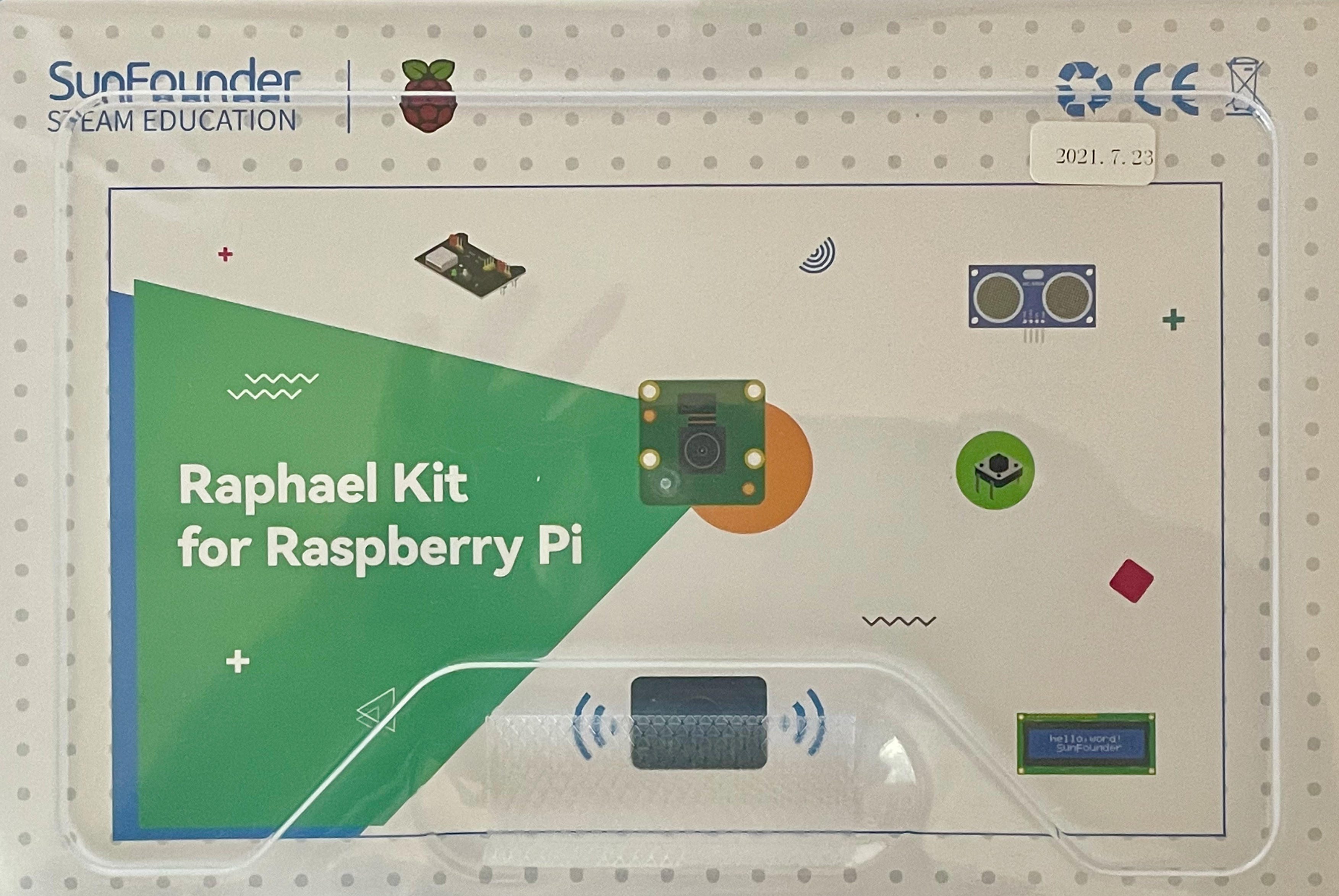
Here’s a simple kit that has all (most?) of the above. The photo of the kit appears to show a shift register, but I can’t be sure. I’m finding the Sunfounder Raspberry Pi Ultimate Starter Kit especially useful. NOTE: The Ultimate Starter Kit and the Raphael Kit are the same product.
You will also need some basic C and Go programming knowledge as well as familiarity with logging on to a Raspberry Pi terminal, or into the desktop GUI that comes with some OS versions. Depending on the approach you take, you may need to connect a keyboard and monitor to the Raspberry Pi. I simply SSH into the Pi. You’ll also need familiarity with how to use an editor like vim or nano.
To compile and run the C program you’ll need the WiringPi library. It’s easy to get:
sudo apt-get install wiringpi
Then test the installation using:
pi@pi-node1:~/go/src/github.com/youngkin/gpio/rgbled $ gpio -v
gpio version: 2.50
Copyright (c) 2012-2018 Gordon Henderson
This is free software with ABSOLUTELY NO WARRANTY.
For details type: gpio -warranty

Raspberry Pi Details:
  Type: Pi 3B+, Revision: 03, Memory: 1024MB, Maker: Sony
  * Device tree is enabled.
  *--> Raspberry Pi 3 Model B Plus Rev 1.3
  * This Raspberry Pi supports user-level GPIO access.
In the above you’ll notice gpio version: 2.50. If you’re using a Rasberry Pi 4, use the instructions given in the Sunfounder Checking the WiringPi.
WiringPi is unique in that it includes a command line tool, gpio, as shown above, that can be used to manage, control, and query the GPIO board. This can be very handy. See the gpio reference for more information on what it can do and how to use it.
If you’re interested in Go development on a Raspberry Pi you’ll need to install the development environment onto the Raspberry Pi. Here’s a simple source that explains how to accomplish this. This source is a little dated, but the only significant issue is with the version of Go to install. The source shows installing Go 1.14.4.linux-arm64.tar.gz and 1.14.4.linuxarmv6l.tar.gz. The current versions are 1.17.1.linux-arm64.tar.gz and 1.17.1.linuxarmv6l.tar.gz. For the Raspberry Pi 3B+ the correct choice will be 1.17.1.linuxarmv6l.tar.gz. The other is intended for 64 bit systems like the Raspberry Pi 4 series. You can find current ARM versions of Go at the Golang download site.
For Go development you’ll also need the go-rpio library.
If you want to veer away from the cookbook style of the Sunfounder docs you’ll need some basic knowledge of Linux . For example, I won’t be explaining what root privileges are.
Information that would have been helpful
The Sunfounder 7-Segment Display project documentation pretty much just jumps into how to wire up the breadboard and the code without mentioning much about the hardware components, especially the shift register. Even the code description was a little confusing given my lack of knowledge about shift registers. I accidentally stumbled across the Sunfounder 7-Segment Python project documentation that did provide some useful information on the 7-segment display, but still no mention of the shift register. This project could easily be done without the shift register, in fact many other articles on 7-segment displays do just that. So why does the project use a shift register? Why not just wire the 7-segment display directly to the GPIO pins? Clearly there’s something to the shift register and I wanted to know what that was. It turns out, for me anyway, that this project is really about shift register with the 7-segment display being merely a tool to visualize how shift registers work. But before we get to shift registers, let’s have a short discussion about 7-segment displays.
What is a 7-segment display?
So what is a 7-segment display? Well, to be pedantic, it has 8 segments if you include the decimal point on the device. That aside, it’s a common device you’re already familiar with having seen them used in everything from clocks to calculators and other devices that need a numeric display. In terms of the physical implementation there are a few details we need to know.
| Pinout diagram | LED Identification diagram |
|---|---|
 |
 |
First of all, the diagram to the above left shows the pinout designations for the 7-segment display. This diagram shows the middle pins on the top and the bottom with a (-) annotation. This designates those pins to be the ground pins for the display. The letters on the remaining pins correspond to the letters in the LED identification diagram on the right. For example, applying power to the ‘A’ pin on the display will light up the LED labeled ‘A’ in the diagram to the right. The letters “DP” stand for decimal point.
For this project we need what is known as a common cathode 7-segment display. This is what the diagram above left is showing (the middle pins on the top and the bottom have a (-) annotation). All this means is that all the negative terminals of the LEDs in the display are connected to a common ground pin. Common anode is the other type, which as you might expect, means all the LEDs’ positive terminals are connected to the same pin.
If you’re using the Sunfounder kit the 7-segment display is a common cathode display. If you got a 7-segment display from another source you might want to verify it’s type. Determining whether a 7-segment display is a common cathode or common anode is fairly easy to do. Paraphrasing from How to set up seven segment displays on the Arduino, which is also the source of the above diagram, the steps are as follows:
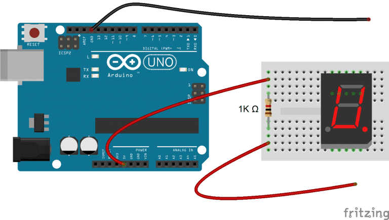
While the above diagram shows an Arduino, hooking it up to a Raspberry Pi is very similar.
- You’ll need the Raspberry Pi 3.3v power pin hooked up to a breadboard.
- Connect the power from the Raspberry Pi as shown above (or to the breadboard’s power bus).
- Connect a resistor between the 2 sides of the breadboard, or from the power bus to one side of the breadboard.
- Connect a jumper wire (red) on the far end of the resistor from the power source.
- Connect a jumper wire (black) to the Raspberry Pi’s GPIO ground pin.
- Connect the black jumper wire (ground) to the middle pin, top or bottom, of the display.
- Connect the red jumper wire (positive) to any of the other pins (except the middle pin!).
- If an LED lights up the display is a common cathode.
- If an LED doesn’t light up
- Disconnect the jumpers from the display
- Connect the red jumper to one of the middle pins, top or bottom
- Connect the black wire to one of the other pins.
- At this point an LED should light up and you’ve verified that the display is a common anode display
- If no LED lights up then double-check your wiring.
This YouTube video shows how to accomplish this using a multimeter instead of wiring up a breadboard as described above.
What is a shift register and what is it good for?
There are several types of shift registers. For this project we’re using what’s known as a “Serial In, Parallel Out” (SIPO) shift register. This type of shift register converts a serial input into a parallel output. For example, several pulses of a signal generated on a single Raspberry Pi GPIO pin can be accumulated by the shift register and then sent as a single parallel output to a 7-segment display. This is exactly what is being done in this project.
So why use a shift register? Well for one, as noted above, it only takes one GPIO pin to drive 8 pins on a 7-segment display (not quite true, this will be explained in more detail farther into the article). Versions of this project without a shift register take 8 GPIO pins to accomplish the same thing. So, one use of a shift register is to conserve GPIO pins. This is especially true of LED displays with a very large number of LEDs that perhaps wouldn’t be usable due to a lack of available GPIO pins. Although this isn’t true of a 7-segment display, some devices only take parallel input. So for this kind of situation, a SIPO shift register is mandatory in converting a serial source into a parallel output.
Shift register anatomy
The 74HC595 shift register has a couple of logical components that are pertinent to this article:
- Input shift register - This is a series of connected flip-flop devices that receive incoming (serial) data on the receipt of each synchronizing clock pulse (more about this later). This register is comprised of outputs that are named in sequence from Qa’ to Qh’, i.e., Qa’, Qb’, …, Qh’.
- Output or storage register - This is another series of connected flip-flop devices that transfer the serial data in parallel to a connected device. This register is comprised of outputs that are named in sequence from Qa to Qh, and Qh’ (more on Qh’ below).
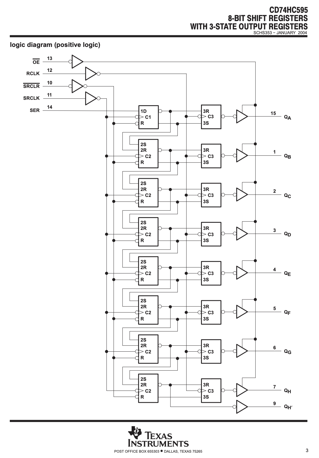
This anatomy is shown graphically in the following, albeit somewhat complex, diagram from the Texas Instruments CD74HC595 8-Bit Shift Registers with 3-State Output Registers datasheet. The first column of 8 boxes to the left, labeled C1 or C2, comprise the input shift register. The second column of 8 boxes to the right, labeled C3, comprise the output shift register. The output register’s output pins can be seen at the far right, labeled Qa through Qh, and Qh’. The input and control channels, as shown by OE, RCLK, SRCLR, SRCLK, and SER in the upper left of the diagram, are discussed in more detail below.
More information pertaining to the Q* names for the registers’ outputs is provided below.
It is a little confusing for the entire device to be called shift register as well as the input component to also be called shift register. To differentiate between the two, if it’s not clear from the context, I’ll make sure to reference which one I’m referring to when the term is used later in the article.
| Pin Diagram | Photo |
|---|---|
 |
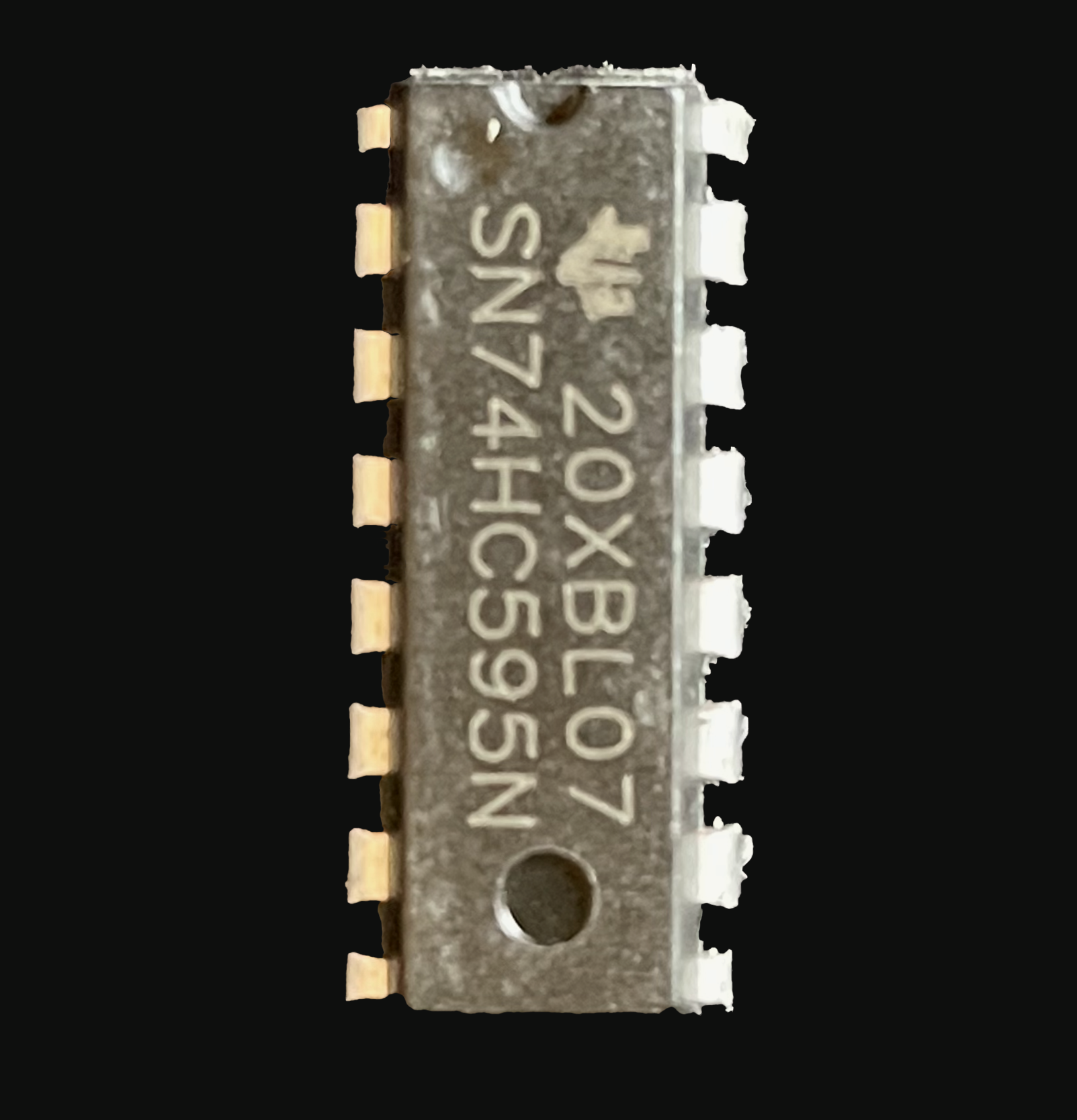 |
The diagram at above left shows the pinouts for a SN74HC595 shift register. The photo at above right is in the same orientation as the pin diagram, namely GND is in the lower left, Vcc is in the upper right, and the “notch” is at the top center. The pins are defined as follows:
- Pin 15 (right side, 2nd from the top), Qa, is the first output pin. Qa is also known as Q0.
- Pins 1-7, Qb-Qh, are the remaining output pins. Notice that there are 8 output pins (including Qa above). Having 8 outputs makes this an 8-bit shift register. Qb-Qh are also known as Q1-Q7.
- Pin 8, GND is the ground pin.
- Pin 16, Vcc, is the power-in pin.
- Pin 14, SER, is the serial input pin. This is the pin that takes the incoming serial data pulses from the Raspberry Pi. This is sometimes referred to as DS, SI, or SDI.
- Pin 11, SRCLK, is the pin that accepts the synchronization signal that indicates 1 bit of data has been transmitted to the SER pin. This type of signal is called a clock. SRCLK stands for shift register clock. SRCLK is also known as sh_cp.
- Pin 12, RCLK, is the pin that accepts the synchronization signal that indicates all 8 shift register bits have been populated and it’s time to transfer the bits, in parallel, to the output/storage register and thereby to the device connected to the output pins, Qa-Qh. RCLK is also known as st_cp or latch.
- Pin 10, SRCLR, is used to clear the current values of the shift register. SRCLR stands for shift register clear. SRCLR is also known as MR. If clearing the shift register is not required it can be connected to the power source which generates a HIGH signal (or 1). To clear the shift register the SRCLR pin is set to LOW (or 0). It must be set back to HIGH before the shift register is functional again.
- Pin 13, OE, is used to block the availability of the output or storage register. The OE pin’s effect is temporary. When it’s set to LOW (0) the data in the output register is accessible. When it’s HIGH(1) the data is not accessible. Setting it from HIGH to LOW makes the data once again accessible. Unlike the SRCLR pin, it does not clear the register. If disabling the output register is not required it can be connected to ground.
- Pin 9, Qh’, is used to daisy chain multiple shift registers. For example, imagine a project that needed to control 16 LEDs in a parallel fashion. In this case a single 8-bit shift register is inadequate, we need 2 that can communicate in some manner. We can get the other required 8 bits from a second 8-bit shift register. To link the 2 shift registers we connect the Qh’ output from the first, to pin 14, SER, on the second shift register. Daisy chaining shift registers is beyond the scope of this project, but you can read more about it on Multiple Shift-out Registers on Arduino - part 1.
Shift register in operation
As stated above, input data is stored in the input shift register. Data is transferred on each pulse of the SRCLK input. When an SRCLK input is received, data on a prior Q*’ pin is shifted to the next Q*’ register in the sequence. When the input shift register has been populated an RCLK signal causes all of the input register contents to be transferred to the output register. The following table illustrates this behavior. To keep things simple, I’m limiting the example to 4 bits, Qa* to Qd*. The input bit sequence will be 1011. The first bit, 1, will be transmitted at t0. The transmitted bits are indicated in parentheses next to the time indication (e.g., t0(1)). The 4 bits become available at the output register on a signal from RCLK at t4.
| SRCLK | t0 (1) | t1 (0) | t2 (1) | t3 (1) | t4 |
|---|---|---|---|---|---|
| Qa’ | 1 | 0 | 1 | 1 | - |
| Qb’ | - | 1 | 0 | 1 | - |
| Qc’ | - | - | 1 | 0 | - |
| Qd’ | - | - | - | 1 | - |
| RCLK | - | - | - | - | 1 |
| Qa | - | - | - | - | 1 |
| Qb | - | - | - | - | 1 |
| Qc | - | - | - | - | 0 |
| Qd | - | - | - | - | 1 |
Notice that in the output sequence of bits, if the output bits are read from Qa to Qd, the bit sequence is reversed. That is, 1101 vs. the input sequence of 1011. This manner of shifting is called Most Significant Bit (MSB) shifting. It starts with the leftmost bit as in this example. This must be kept in mind or unexpected results may occur. It is possible to shift in a more intuitive way, Least Significant Bit (LSB). To do this the shifting must start with the least, or rightmost, input bit. In C and Go, MSB shifting is done using the << shift operator. LSB shifting is done by using the >> shift operator. The impact of shift method will become more obvious when we get to how the shift register (not the input shift register) is used in conjunction with the 7-segment display. See Wikipedia for more about MSB and LSB.
As noted previously, I simplified things a little bit when I stated above that only one Raspberry Pi GPIO pin is needed to drive the 8 LED segments in the 7-segment display. The one pin I identified is used for the SER (serial data in) pin. A minimum of 2 more are needed; 1 for the SRCLK pin and the other for the RCLK pins. As shown above these are required to advance the clock on the input shift register and transfer data from the input shift register to the output register respectively. So that’s now 3 pins to drive the 8 LEDs on the 7-segment display. This is still a good tradeoff. But 2 more GPIO pins are needed if the SRCLR and OE pins are needed. So now that’s 5 GPIO pins to drive 8 LED segments. Still a net gain of 3 pins. However, the savings become even greater when shift registers are daisy-chained as discussed above. Without requiring additional GPIO pins it is possible to control 16 or even more LEDs from those 5 GPIO pins. The savings become more significant as more devices, e.g., LEDs, need to be controlled.
How does this project use the shift register and 7-segment display?
This project uses the shift register component to capture serial input, accumulate it until 8 bits are written, and then make it available to the output register. Since the shift register component is wired to the 7-segment display, the contents of the output register are made available to the 7-segment display, controlling what is ultimately displayed. The details of the pin connections from the shift register component to the 7-segment display pins, coupled with the shift method used, MSB in this case, dictate what LEDs will be illuminated on the 7-segment display. The following table provides the specific pin assignments as well as what the final values at the output register will be given that the input number is 0x3f, 0011 1111, is used with MSB shifting.
| 74HC595 pin | 7-segment display pin | Final value |
|---|---|---|
| Qa | A | 1 |
| Qb | B | 1 |
| Qc | C | 1 |
| Qd | D | 1 |
| Qe | E | 1 |
| Qf | F | 1 |
| Qg | G | 0 |
| Qh | DP | 0 |
Using the diagrams below we can ascertain what number will be displayed at the 7-segment LED.
| Pinout diagram | LED Identification diagram |
|---|---|
|
|
7-segment display pins A-F will have the value 1, G and DP will have the values 0. Mapping this to the above LED Identification diagram we can see that the number displayed will be 0.
Setup and Code
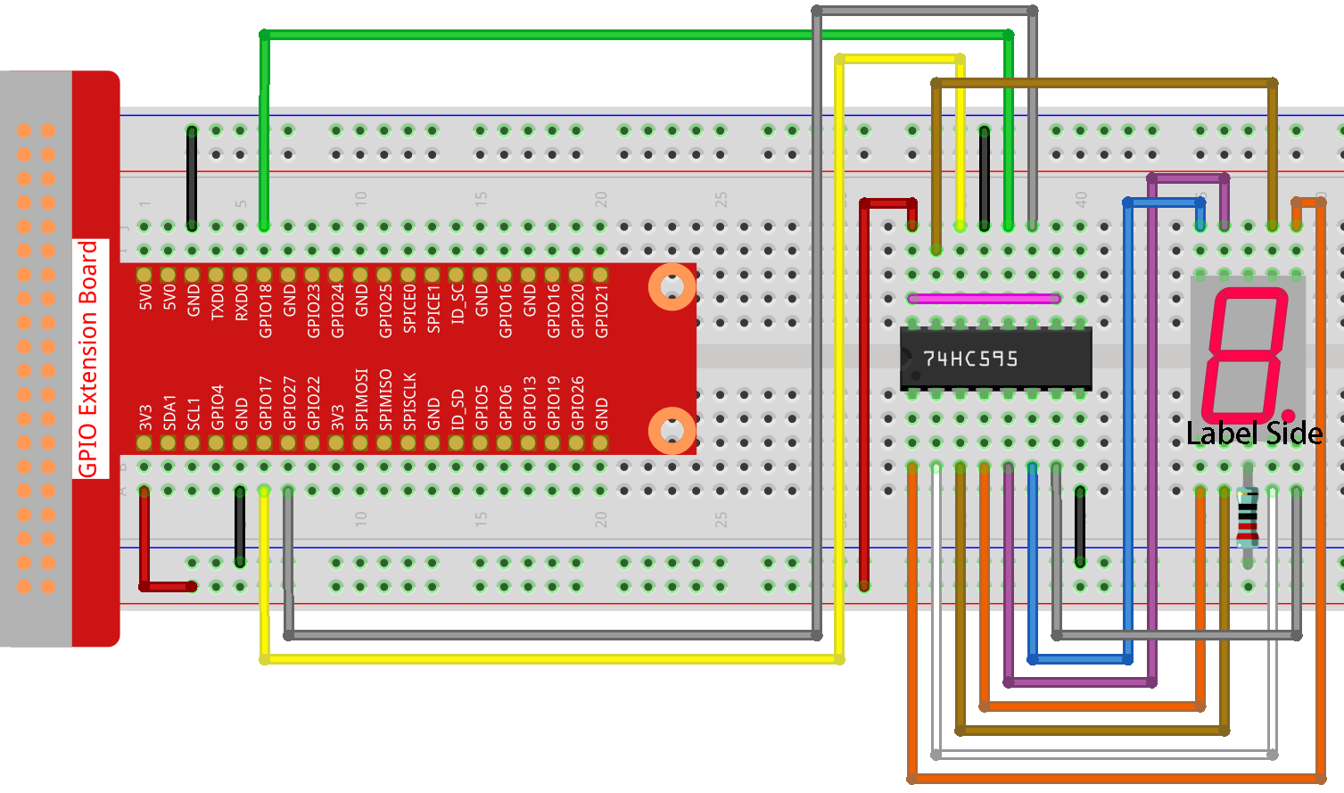
The breadboard should be wired as illustrated in the above diagram (as indicated in the Sunfounder 7-Segment Display project documentation). One very important thing to note, something that I spent way too much time debugging, is that the resistor connecting the ground pin on the 7-segment display must be connected to the ground or negative bus on the breadboard. In all my prior projects I’ve connected the resistor to the positive breadboard bus. I initially missed this detail and the 7-segment display didn’t display anything. One other thing I got wrong on the initial wiring is that I had the 74HC595 output register pins connected incorrectly to the 7-segment display. This is easy to do. I debugged this by noting which LED segments lit up for which expected number. After going through several numbers it became apparent that I had the ‘G’ and ‘E’ pins on the 7-segment display reversed.
If you’re unfamiliar with breadboards and breadboard diagrams this breadboard tutorial should be helpful.
Shift Register/7-Segment Display in C
This code is quite different from the Sunfounder code. This is because I chose to add several capabilities including:
- Support for an interrupt handler. This will gracefully exit the program by clearing the input shift register thereby turning off all the LEDs. The Sunfounder program will leave the LEDs in whatever state they were in when that version exits.
- It supports setting both the SRCLR and OE shift register pins.
- It adds support for illuminating the decimal point in the 7-segment display.
- It add several functions that provide the ability to test different capabilities of the 74HC595 shift register including using the SRCLR and OE pins.
- It accepts user input from the keyboard allowing the user to specify how they’d like the program to drive the shift register and hence the LED. This includes things like clearing the input shift register, disabling and reenabling the output register as well as writing all hexadecimal digits/decimal point as well as writing an
8.to the display.
Most of this is pretty well explained by the embedded comments, but I’ll mention of few highlights.
Lines 12 and 13 provide information on how to build and run the program.
Lines 27 and 28 define the GPIO pins that drive the SRCLR and OE pins respectively. Note that the GPIO pin numbers are the WiringPi pin numbers. If you decide you want to see this behavior in action, wire pin 24 to the SRCLR shift register pin, and wire pin 29 to the OE shift register pin instead of positive and ground respectively.
Lines 32 and 33 define an array, SegCode, that contains the hexadecimal numbers that will be shifted into the shift register in order to display a number that matches the index of a particular number in the array. For example, to display an 8 SegCode[8] should be used. Note that these numbers reflect the use of the MSB form of shifting. The numbers would be different if the LSB shifting form were used. For example, the number to use to display 0, as shown on line 32, is 0x3F (0011 1111). To display 0 using the LSB method the hex number 0xFC(1111 1100) and the C right-shift operator, >>, should be used.
This next code snippet shows the initialization of the shift register. In a nutshell, all the pins we’re using are placed in OUTPUT mode so we can write to them. Next, all pins except for the SRCLR pin are set to LOW (0). Recall that the SRCLR pin must be set to HIGH for the shift register to be operational.
The alternative to pin mode OUTPUT is PWM (Pulse Width Modulation). Since PWM simulates lower voltages by rapidly pulsing the associated pin it’s not suitable for use with shift registers. Recall that a pulse to the SRCLK and RCLK pins represents a clock advancing. Using PWM, and the resulting rapid pulsing, would interfere with the clocks advancing in a reliable manner.
This code snippet demonstrates 2 methods of turning off all the LEDs in the 7-segment display. Specifically, it shows how to use both the SRCLR pin and writing zeros to all the input shift register bits to clear the input shift register that will result in the 7-segment display showing nothing.
In shiftRegClr, lines 1 through 11, note the use of the RCLK pin on lines 4 and 6. The clock signal to that pin must be pulsed, i.e., set to HIGH followed by LOW, in order to make the input shift register contents available to the output register. Also note that the SRCLR pin needs to be reset to HIGH after the operation to reenable the shift register.
Lines 16 through 28 show the method of writing zeros to all the input shift register bits to clear the input shift register (zeroClear()). This is functionally equivalent to using the SRCLR method, they both set the input shift register bits to 0. It does take a lot more effort however. The for loop in lines 18 through 23 shifts a zero into each bit of the input shift register. It repeats the process 8 times, advancing the SRCLK with each write, to fill the input shift register bits. Lines 20 and 22 send the SRCLK pulse to advance the input shift register bits. Strictly speaking, it’s not necessary to shift the 0 and & it to 0x80 on line 19. It would be sufficient to merely write 0 to the SDI pin. However, it is necessary to use this method of writing to the SDI pin write any other number, e.g., 0x3F into the input shift register.
As with shiftRegClr() above, lines 25 and 27 toggle the RCLK pin to transfer the bits to the output register.
This next code snippet demonstrates how to light up all the LEDs, including the decimal point, as well as toggling the OE pin to temporarily disable the output register.
Lines 3 through 15 show writeAllOnes(). It’s implemented almost exactly like zeroClear() above. The one notable exception is that it doesn’t left-shift the 1 and & it to 0x80 before writing it to the pin. This demonstrates that when all input shift register bits will have the same value, i.e., 1 or 0, it’s not necessary to do this. It does however repeat the process of writing to the pin 8 times, advancing the SRCLK clock after each write.
Lines 22 through 29 implement oeToggle(), which toggles the OE pin to HIGH (1) and then LOW again. There’s a 1 second delay between the writes to ensure that the effect is visible. Recall that setting to OE pin to HIGH is how the output register is disabled. From the observer’s perspective, the 7-segment display will turn off for 1 second and then be restored to whatever was being displayed prior to the toggling. It’s up to the calling function to decide what is displayed on the 7-segment display prior to calling this function.
hc595_shift() is responsible for shifting the various bits of the input number, dat, into the input shift register. With the exception that the input number is variable based on what the value of dat is, the function is implemented exactly like zeroClr() above. In fact, both zeroClr() and writeAllOnes() can, and probably should have been, implemented using hc595_shift().
For those that might have trouble imagining how the << works in conjunction with the & operator, like I did, here’s a short example using 0x3f or 0011 1111 as an example. Note that the order of precedence of the operations is that << happens first followed by the &.
i |
dat after shift |
dat & 0x80 |
result written to the SDI pin |
|---|---|---|---|
| 0 | 0011 1111 | 0011 1111 & 1000 0000 | 0 |
| 1 | 0111 1110 | 0111 1110 & 1000 0000 | 0 |
| 2 | 1111 1100 | 1111 1100 & 1000 0000 | 1 |
| 3 | 1111 1000 | 1111 1000 & 1000 0000 | 1 |
| 4 | 1111 0000 | 1111 0000 & 1000 0000 | 1 |
| 5 | 1110 0000 | 1110 0000 & 1000 0000 | 1 |
| 6 | 1100 0000 | 1100 0000 & 1000 0000 | 1 |
| 7 | 1000 0000 | 1000 0000 & 1000 0000 | 1 |
| 8 | 0000 0000 | 0000 0000 & 1000 0000 | 0 |
The last entry, i = 8, is what would happen if dat was shifted 9 times instead of 8. This was included just to make it clear that dat has been shifted 8 bits to the left leaving all 8 bits set to 0.
Most of the functions in the above code snippet merely setup the test by setting the display to 8, and then delegate the behavior to the functions that we saw implemented above (e.g., shiftRegCLr()). Instead of merely displaying an 8, testWriteNum() will rotate through all the hexadecimal numbers and decimal point.
Finally, this code snippet implements the main() and interruptHandler() functions.
Line 3 registers a signal handler, interruptHandler(), with interest in the SIGINT signal. SIGINT is what will be generated when ctl-C is entered at the terminal.
Lines 6 through 9 initialize the WiringPi library, exiting if the initialization fails.
Line 16 prompts the user for what behavior they’d like to see demonstrated.
Lines 17 through 25 first read the terminal input from the user and populate a null terminated string with the results. The code doesn’t care for any characters that might have been entered except the first character. Any additional characters between it and the newline will be ignored.
Line 26 frees the memory allocated by getline() on line 19. This is necessary to avoid memory leaks. Don’t worry if you don’t understand this. It’s not important to what’s being demonstrated in this program. If you’re interested, investigate memory allocation in C including how memory is allocated (malloc), how it’s freed (free), why this is important, and finally the operation of the getline() function. Otherwise just remember it’s required.
ASIDE: strictly speaking it’s not actually required in this program as the resulting memory leak is likely to be trivial in normal use. At a minimum it’s bad form to not
freeall allocated memory when it’s no longer needed. At worst, the program can fail in various ways once all available memory has been allocated. So, callfreewhen the memory associated with a variable likelineis no longer needed.
Wikipedia has a very detailed discussion about memory allocation and management.
Lines 28 through 56 detect which option the user chose and call the function associated with that option. The entire process described from line 15 onwards is repeated until the user chooses the (q)uit option.
Lines 63 through 67 register the signal handler that will gracefully exit the program if ctl-C is entered at the terminal. It calls toggle8() which briefly displays an 8 before turning off all the LEDs in the 7-segment display.
Shift Register/7-Segment Display in Go
The Go program is very similar to the C version. There are some minor differences in the implementation and the runtime output. Some of these differences are due to structural differences between the languages as well as differences in coding conventions. The snippets below represent most, but not all of the program. I left out some of the boiler plate and whitespace.
There are 4 major parts to this snippet. The first is the definition of the segcode variable on line 3. It serves the same purpose as SegCode in the C program, namely defining the values to be left-shifted into the shift register. One thing of note is that, as with the C version, these values are dependent on the use of Most Significant Bit shifting (MSB). For convenience, here’s the explanatory text from the C version:
SegCode… contains the hexadecimal numbers that should be shifted into the shift register in order to display a number that matches the index of a particular number in the array. For example, to display an 8SegCode[8]should be used. Note that these numbers reflect the use of the MSB form of shifting. The numbers would be different if the LSB shifting form were used. For example, the number to use to display 0, as shown on line 32, is0x3F(0011 1111). To display 0 using the LSB method the hex number0xFC(1111 1100) and the C right-shift operator,>>, should be used.
Second, lines 7-13, in main(), initialize the go-rpio library. Line 13 guarantees that the resources held by the go-rpio library will be released on program termination.
Third, lines 15-20, create the go-rpio rpio.Pin objects that are manipulated by the rest of the program.
Finally, lines 22-35, define a signal/interrupt handler to catch ctl-C inputs from the terminal. This is needed to gracefully exit the program if the user enters ctl-C at the keyboard. A key point to notice in this snippet is the use of the channel named stop. The signal/interrupt handler runs in its own goroutine (line 35). At this point there are 2 goroutines running, the main() goroutine and the goroutine associated with the signal/interrupt handler. They are run and scheduled independently and as a result control can shift from one goroutine to another in arbitrary and unpredictable ways. In order to gracefully shutdown the program they must both be stopped in a controlled manner. Otherwise exiting the program would result in unpredictable behavior. For example, at program exit the 7-segment display might still have some illuminated LEDs. Synchronizing program exit using the stop channel prevents this from happening. See the Tour of Go lessons on Goroutines and Channels for a quick introduction to goroutines and channels. Don’t worry if you don’t quite understand all this, concurrency in Go is an advanced topic. Mostly I just wanted to provide a high level explanation of why the code is written this way.
The program comments provide additional detail. The rest of main() is in the following snippet.
The rest of main() as shown above handles prompting the user about what capability they’d like to see demonstrated is fairly self-explanatory. One thing to point out though is the for/select loop starting in lines 2-8. for/select is a common pattern used in Go programs. It’s use here goes back to the the prior discussion about the stop channel. The select part of the for/select pattern is listening on the stop for the message indicating this goroutine should exit. Notice the select had 2 case choices. The first is for listening to the stop channel. If a message is received the for loop, and program, will exit. If no message is received then control will immediately pass to the default case, continuing with normal program flow. In the default case the user is prompted, in lines 18-57, for their choice which will result in one of the test functions being called.
There are 3 parts to this next code snippet. The first is the creation of the go-rpio rpio.Pin objects that represent the logical connection to the shift register’s physical pins. The GPIO/BCM pins 17, 18, 27, 19, and 21 are used for the SDI, RCLK, SRCLK, SRCLR, and OE pins respectively.
The second part sets the pins to OUTPUT mode so that they can be written to.
The final part sets the voltage on the pins to their initial values. Note the the SRCLR pin is set to HIGH. This is required in order for the shift register to work. In later code snippets we’ll see that clearing the input shift register is accomplished by setting the SRCLR pin to LOW to clear the input shift register, and then back to HIGH to reenable the normal operation of the shift register.
This code snippet shows the implementation of the test functions that are called in response to users’ choices regarding what capability they’d like to see demonstrated.
This code snippet shows the implementation of the function that’s the heart of the program, hc595_shift(), which does the actual writing to the input shift register. The comments provide a good detailed explanation of what the function does.
This final code snippet shows the implementation of 2 helper functions and the signal/interrupt handler. The first helper function, writeNums(), writes the actual data needed to illuminate the hexadecimal numbers on the 7-segment display. The second, shiftRegClr(), shows how to use the combination of the SRCLR and RCLK pins to clear the shift register ultimately clearing the 7-segment display. Note that, as described above, the SRCLR pin needs to be set back to HIGH in order to reenable the shift register.
In shiftRegClr, lines 12 through 18, note the use of the RCLK pin on lines 14 and 16. The clock signal to that pin must be pulsed, i.e., set to HIGH followed by LOW, in order to make the input shift register contents available to the output register. Also note that the SRCLR pin needs to be reset to HIGH after the operation to reenable the shift register.
Finally, the signalHandler() function catches the signal from the OS (line 23) via the sigs channel. Then on (line 25) it closes the stop channel. A side effect of closing a channel is a notification is sent to all listeners on the other end of the channel. This is a common pattern in Go. Finally it clears the shift register, releases go-rpio resources (line 28). Line 30 releases the resources held by the go-rpio library. Finally, the program exits on line 32.
Summary
This article has covered quite a bit of ground. If you’ve been following my series starting with the Raspberry Pi GPIO in Go and C - Blinking LED project, you’re already familiar with using GPIO to drive LEDs. You might agree that the Sunfounder 7-Segment Display project didn’t really add to your knowledge of GPIO and LEDs that hasn’t already been covered in previous projects. So this is why, for me anyway, this project is really about learning shift register fundamentals and using them in a non-trivial way.
This article covered several interesting things:
- It demonstrated wiring up a relatively complex circuit on a breadboard. As I did, you might have made some mistakes along the way that gave you some useful knowledge of how to debug circuits.
- Through an academic discussion and hands-on practice you’ve learned quite a bit about shift registers and what they can be used for.
- Despite my somewhat trivializing the use of LEDs in this project, this project did shed light on how to use LEDs in a more realistic manner. Controlling an individual LED is interesting, but being able to control an array of LEDs in parallel and display digits on that array is a big step forward. You also learned that there are 2 types of 7-segment displays, common anode and common cathode.
Comments and questions about this article are welcome.
References
- The Sunfounder 7-Segment Display project documentation.
- The Sunfounder 7-Segment Python project contains some additional information not available in the C version of the project.
- Raspberry Pi GPIO Pinout diagram including the physical board pin numbers, the BCM/GPIO pin numbers, and the WiringPi pin numbers.
- Shift Registers: Serial-in, Parallel-out (SIPO) Conversion is a good resource for getting a detailed introduction to shift registers in general, and the 74HC595 shift register in particular.
- Texas Instruments CD74HC595 Datasheet contains some interesting information including a timing diagram.
- How to set up seven segment displays on the Arduino provides an example of a 7-segment LED project that doesn’t use a shift register. It also has some other useful information such as how to determine whether a 7-segment display is a common cathode or common anode display.
- WiringPi library for C
- WiringPi website
- go-rpio library for Go
- Other articles in my Raspberry Pi GPIO series
- The gpio repository containing the code for this article
- How to setup a new Raspberry Pi from scratch
- How to use a breadboard