Contents
This is the seventh article in a series that explores GPIO programming on a Raspberry Pi. It describes how to control Serial Peripheral Interface (SPI) peripherals such as the MAX7219 LED Dot Matrix Display Module.
Overview
There are 2 approaches to reading this article. The first is to focus only on the SPI and dot matrix display aspects of the article by skipping the Controlling the MAX7219 - direct interaction with the BCM2835 section. The second approach involves also learning how to control SPI peripherals by directly accessing the SPI register set instead of using a 3rd party library. This requires reading the Controlling the MAX7219 - direct interaction with the BCM2835 section.
If the second approach is taken, then the Raspberry Pi GPIO - Introduction To Programming Broadcom BCM2835 ARM Peripherals article should be considered a prerequisite of this article. That article introduces key techniques for directly controlling peripherals connected to the BCM2835, or more generally, the GPIO interface on the Raspberry Pi. Those key concepts include:
- BCM2835 I/O functions
- BCM2835 addressing
- Using BCM2835 registers
If all you’re interested in is learning SPI without learning the details of programming the BCM2835 then the first approach is best.
The following topics will be covered:
- Prerequisites - describes the hardware and software libraries you’ll need for this article.
- Overview of the Serial Peripheral Interface (SPI) - provides an introduction to the SPI protocol and the MAX7219 Dot Matrix Display Module.
- Using the BCM2835 board to control the MAX7219 Dot Matrix Display Module - provides the details, including code, for controlling the MAX7219. It also includes a subsection that describes directly interacting with the SPI register set on the BCM2835.
- Summary - summarizes the important concepts covered in this article.
- References - provides a list of references I found helpful and some that were used in the creation of this article.
Prerequisites
If you don’t have one, you’ll need a Raspberry Pi. I used a Raspberry Pi 3B+ with the ‘stretch’ or later version of the Raspbian OS. The BCM2835 library referenced below supports Raspberry Pi models 1 through 4.
Next you’ll need is a breadboard, some jumper wires, and a MAX7219 Dot Matrix Display. You should also consider getting a 40 pin female to female with a T-Type adapter to attach the GPIO outputs to the breadboard. You can use only jumper wires, but the adapter will make things easier and will help prevent damage to the GPIO pins on the Raspberry Pi. If you elect not to buy the 40 pin cable with T-Type adapter you’ll need to buy male-to-female jumper wires. However, a full electronics kit for a Raspberry Pi doesn’t cost much more than these 4 components. I recommend buying the Sunfounder Raspberry Pi Ultimate Starter Kit.
You will need some basic C programming knowledge as well as familiarity with logging on to a Raspberry Pi terminal, or into the desktop GUI that comes with some OS versions. Depending on the approach you take, you may need to connect a keyboard and monitor to the Raspberry Pi. I simply SSH into the Pi. You’ll also need familiarity with how to use an editor like Vi or nano. And you’ll need basic familiarity with the Linux command line.
Finally, you’ll need to clone or fork my GPIO repository as it contains underlying library code used to access GPIO capabilities on the BCM2835. As mentioned in other sections, this library code is based on the BCM2835 C library developed by Mike McCauley.
SPI (Serial Peripheral Interface) Overview
SPI is used to send data serially to a peripheral that can accept or requires data in parallel. This is helpful because a relatively large set of parallel inputs can be written to using just 3 GPIO pins, excluding the power (VCC) and ground (GND) pins. If SPI wasn’t used, one GPIO pin would be required for each parallel input. This could easily be prohibitive since pins are a limited resource. Let’s see how this works with an example.
The diagram above shows the MAX7219 LED Dot Matrix Display. It’s commonly used to display arbitrary shapes such as letters, numbers, and smiley faces. In addition to the MAX7219, SPI can be used to control a variety of peripherals to display images, take input from touchscreens, and interact with various sensors. Wikipedia has a good article describing SPI in more detail.
The MAX7219 controls an 8x8 matrix of LEDs. Controlling an LED requires 1 pin excluding power or ground. An 8x8 LED matrix has 64 LEDs. This number is well in excess of the 26 or 40 GPIO pins available on a standard Raspberry Pis. As explained below, utilizing SPI requires considerably fewer GPIO pins.
The MAX7219 has the following input pins:
- DIN - this is the serial data input pin.
- CS - This is commonly called a chip select (CS) or chip enable (CE) pin, or occasionally slave select (SS).
- CLK - This pin connects to a clock pin on the Raspberry Pi that synchronizes data transfers between the Raspberry Pi and the MAX7219.
There are 2 more pins that aren’t used to control the MAX7219.
- VCC - This is the power-in pin. It connects to a power source on the Raspberry Pi, usually a 5 volt source.
- GND - This is the ground pin. It connects to a ground pin of the Raspberry Pi.
A minimum of 3 GPIO pins are required to connect from the Raspberry Pi to the MAX7219, specifically to the DIN, CS, and CLK pins. A Raspberry Pi can control all 64 LEDs in a cost efficient (pin-wise) manner using only these three pins. The usual approach is to use the SPI specific Raspberry Pi pins that can drive the DIN, CS, and CLK pins. These 3 pins are named:
- (SPI)MOSI - This stands for Master Out Slave In. The MOSI pin will be connected to the MAX7219 DIN pin and is used to send a serial data signal to the MAX7219 (or any SPI peripheral).
- (SPI)SCLK - This stands for SPI Clock. This pin will be connected to the MAX7219 CLK pin. It is used as the source of the clock signal used to synchronize the data transfer between the BCM2835 and the MAX7219 (or any SPI peripheral). The data transfer will occur when both the MOSI pin and the SCLK pin are set to HIGH.
- (SPI)CS or (SPI)CE - These stands for Chip Select or Chip Enable. In either case, setting the pin to LOW directs the MAX7219 to accept data as described in the previous bullet.
I reluctantly use the terms “master” and “slave”. However these terms are used in all of the documents I’ve read on SPI. I’ll continue to use them in order to avoid confusion.
The SPI capability on the Raspberry Pi may require as many as 5 GPIO pins. The 2 additional pins are:
- (SPI)MISO - This stands for Master In Slave Out. This pin allows for the MAX7219 (or any SPI peripheral) to send data back to the BCM2835.
- (SPI)CS or (SPI)CE - This is a second chip select/chip enable pin. Having a second CS/CE pin allows the BCM2835 to control 2 SPI peripherals. As stated above, when the CS/CE pin is set to LOW the SPI peripheral will accept data from the BCM2835. So by setting one of the CS/CE pins to HIGH and the other to LOW we can control which slave can receive and send data. The article Using Multiple SPI Slave Devices with the Raspberry Pi provides more information about how the 2 CE/CS pins are used. The following schematic illustrates how utilize 2 CE/CS pins:
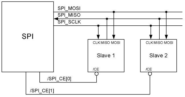
In the image above this schematic you may have noticed the 5 pins on the right-hand side of the MAX7219. These pins output the signals on the corresponding input pins to other MAX7219s. This allows more than two MAX7219s to be “chained” together to create larger displays, e.g., 128 LED or 256 LED displays. This process is called daisy-chaining. This can be done by connecting the output pins on the primary SPI peripheral to the corresponding input pins on the next peripheral in the chain. Daisy chaining can be used to display multiple characters on a logically larger LED matrix, or to create scrolling displays. This Arduino forum thread provides a high level explanation about how to accomplish this. News ticker with three MAX7219 8×8 dot led matrix devices is the best article I could find for implementing a specific project. However, it describes how to accomplish this with Sketch (a way to write Python based code snippets), not C. Between these 2 sources there might be enough hints about how to accomplish this using C. I may write a future article that describes how to do this in C.
It is possible to purchase LED matrix modules that are larger than 8x8 which avoids having to manually daisy-chain multiple devices.
The primary SPI interface on the BCM2835, SPI0, is implemented on GPIO pins 7-11. Pins 7 & 8 are the 2 CE/CS pins available on the BCM2835. Pin 9 is MISO, 10 is MOSI, and 11 is the clock (SPICLK/SCLK). The BCM2835 has 2 auxilary SPI interfaces, SPI1 (AKA AUX_SPI0) and SPI2 (AKA AUX_SPI1). From the BCM2835 ARM Peripherals Guide, SPI1 is available on pins 16-21 and SPI2 on pins 35-39. These auxilary interfaces are available via the AUX I/O function.
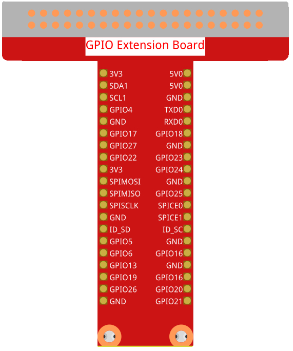
The following diagram shows a GPIO extension board frequently used to connect the BCM2835 GPIO pins to a breadboard (if you’re not familiar with breadboards there’ll be more on them later). The pins are labeled with their GPIO pin numbers or the I/O function (e.g., SPI) they support. Note the SPI pins are labeled on the board using the same terms as above:
The following is a timing diagram that shows the actual signals being sent to the MAX7219 dot matrix display. It’s a screenshot from the PulseView/sigrok logic analyzer application. I used an inexpensive logic analyzer device to capture the signals displayed in PulseView.
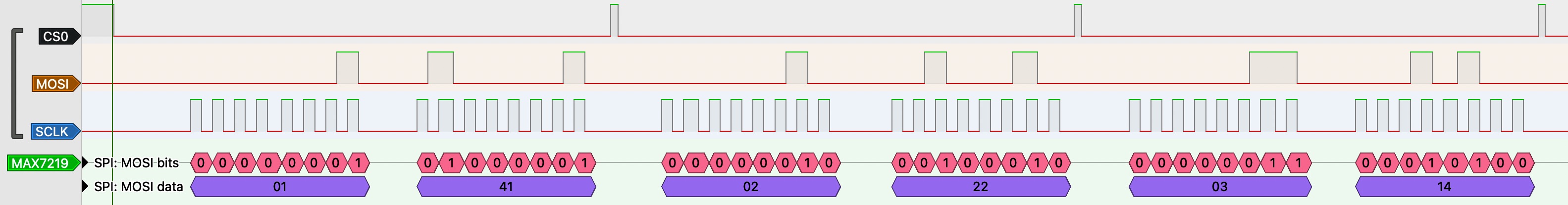
This diagram shows the values for the first 3 rows of the LED matrix for the letter “Y”. Here’s how to interpret it:
-
There are 5 rows/lines going across from left to right labeled CS0, MOSI, SCLK, MAX7219/SPI MOSI bits, and MAX7219/SPI MOSI data. The top three lines are the actual digital signals. Spikes indicate a HIGH signal. The bottom 2 lines are a SPI specific decoding from the 3 line signals above. MAX7219/SPI MOSI bits displays the bit values, 0 (LOW) or 1 (HIGH), associated with the signals above. MAX7219/SPI MOSI data represents the hexidecimal values for the bit values above.
-
CS0 is the chip select line. It’s hard to see, but at the far left of the diagram it starts out set to HIGH. It’s set to LOW where the vertical line appears. This indicates the data transmission to the SPI peripheral attached to CS0 is about to start. While this signal is set to LOW the following happens:
- The SCLK line pulses between HIGH and LOW 16 times while CS0 is set to LOW. This is the timing signal that, when set to HIGH, indicates to the SPI peripheral to accept the current value on the MOSI line.
- For the first 7 pulses of SCLK the MOSI line is set to LOW. Just prior to the 8th pulse the MOSI line is set to HIGH.
- The MAX7219/SPI MOSI bits line shows the binary interpretation of the combination of the SCLK and MOSI lines. Consistent with the first 7 pulses of the SCLK line the MOSI line is interpreted as zeros (0). The 8th bit is interpreted as a 1. So the binary value of the 8 bits sent is
0000 0001. - The MAX7219/SPI MOSI data line shows the hexidecimal interpretation which is
0x1.
The second 8 bits sent while the CS0 line is set to LOW are 0100 0001 which is the hex number 0x41.
The MAX7219 shift register is 16 bits wide. So each data transmission consists of 16 bits, which is what we see in the timing diagram above. 16 bits are transmitted while the CS0 line is set to LOW. For the MAX7219 the first 8 bits are the address of the register that will be set. The value used to populate this register is sent in the next 8 bits. So this first data transmission sets the the register located at offset 0x1 to the value 0x41. The register at offset 0x1 controls the first/top row of the dot matrix module. Notice that there are 8 LEDs in each row. Each LED corresponds to a bit in the binary value contained in the register. That value is 0x41, 0100 0001, which will cause the first row of the LED to look like this (-s are 0, *s are 1):
-*-----*
The next set of 8 bits is 0000 0010 which equates to 0x2. So the value in the 2nd 8 bits will be written to the register at offset 0x2, which corresponds to the 2nd row of 8 LEDS in the dot matrix display. The binary value of the next 8 bits is 0010 0010. The target register will be set to this value. After this transmission the first 2 rows of the LED matrix look like this:
-*-----*
--*---*-
And the next set of 16 bits have the values 0000 0011 and 0001 0100. The first 8 bits are the address of the target register. Which, following the pattern above, specifies the target register is at offset 0x3 which corresponds to the 3rd line of the LED matrix. After the second 8 bits are written to the register the LED matrix will look like this:
-*-----*
--*---*-
---*-*--
The next 5 sets of 16 bits, not shown in the diagram above, specify registers 0x4 through 0x7, corresponding to the remaining rows of the LED matrix. The values written to those registers, 0000 1000, result in the following pattern which represents the letter “Y”.
-*-----*
--*---*-
---*-*--
----*---
----*---
----*---
----*---
----*---
The next section will provide some additional details about the SPI protocol and how to program the MAX7219.
Setup and Code
The diagram below illustrates how to wire the breadboard to work with the MAX7219 LED dot matrix module example. If you’re unfamiliar with breadboards and breadboard diagrams this breadboard tutorial should be helpful.
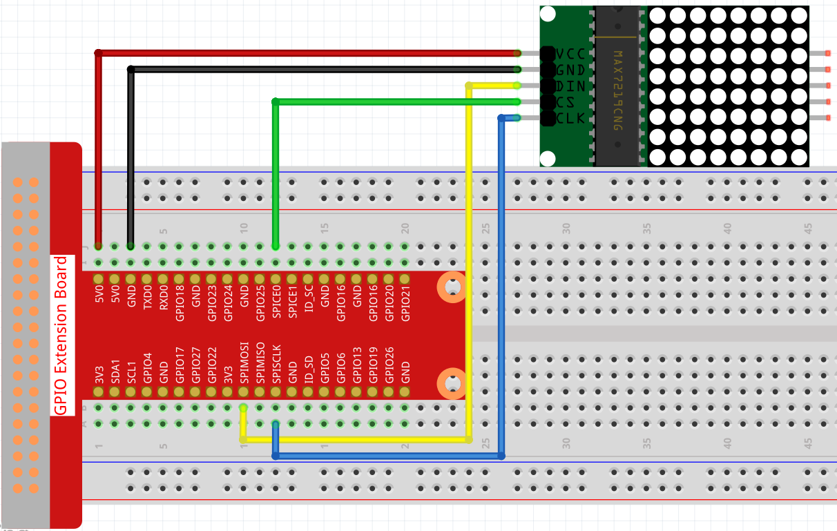
The yellow wire is connected to the SPIMOSI pin (GPIO pin 10) on the Raspberry Pi and the DIN pin on the MAX7219. The blue wire is connected to SPISCLK or SCLK (GPIO pin 11) on the Raspberry Pi and the CLK pin on the MAX7219. The green wire is connected to SPICE0 or CE0 (GPIO pin 8) on the Raspberry Pi and the CS pin on the MAX7219. The red and black wires are connected to 5 volt power/VCC and ground/GND respectively.
The next section will describe the main program that controls the MAX7219. The section following that describes the code that directly controls the I/O functions using the BCM2835 registers.
Controlling the MAX7219 - main program
I mentioned earlier that there are 2 approaches to reading this article. The first approach, the simplist, just involves reading this section. The next section, Controlling a dot matrix display - interacting with the BCM2835, is more advanced and may be skipped.
The code in this section and the next references functions prefixed by bcm_. All of these functions, with very minor changes, were taken from the BCM2835 C Library written by Mike McCauley. When using that library with this code simply substitute all instances of bcm_ with bcm2835_. The bcm_ funcs were created so I could add explanatory comments and to make the BCM2835 code more easily accessible in this article. The bcm_ functions are described in more detail in the following section.
Global variables
This first code snippet shows how to create a character to be displayed on the MAX7219 dot matrix display module. The 2 dimensional matrix disp1 contains a set of rows, NUM_CHARS, each of which define a particular character to be displayed. Each column in the matrix, MATRIX_ROW, defines which LEDs in a single MAX7219 LED row to turn on in the dot matrix display module. The MAX7219 display module is an 8X8 array of LEDs. In the code snippet above the matrix contains 3 rows with 8 columns. The first cell at disp1[0][0] contains the hex value 0x3C. This defines which LEDs to turn on in the first row, of 8 rows, of the display module. 0x3C translates to 0011 1100. Each digit specifies which LED in the row will be turned on. 0x3C specifies that the middle 4 LEDs in the first row of 8 LED rows will be turned on. disp[0][1] contains the hex value 0x42 which converts to the binary number 0100 0010 which specifies that the 2nd and 7th LEDs in the second row of 8 LED rows will be turned on. The dot matrix display will look like this after these 2 cells are displayed:
--****--
-*----*-
LED cells with -s are turned off, cells with *s are turned on. Once all 8 cells from disp1[0][0] to disp1[0][7] are displayed the following character, a zero, will be displayed on the dot matrix module:
--****--
-*----*-
-*----*-
-*----*-
-*----*-
-*----*-
-*----*-
--****--
The remaining disp1 rows define the rest of the characters and shapes that will be displayed by the program.
The Sprint Generator for LED Matrix 8x8 is a tool that helps generate the hex numbers needed to cause an LED matrix to display a given shape.
main()
This next code snippet shows the code for the main function. Each of the significant lines will be explained below the snippet.
Line 1 explains that the GPIO pins are hardcoded. This is because the program is using the SPIO interface. The other 2 interfaces, SPI1 and SPI2 are auxilary SPI interfaces. Section 2.3, page 20, of the The BCM2835 ARM Peripherals guide states the following:
The two universal SPI masters are secondary low throughput SPI interfaces. … The universal SPI master has been developed to work even with the most ‘non-standard’ SPI devices.
Reading between the lines, ‘secondary’, low-throughput’ and ‘non-standard’ don’t seem to be attributes we want to work with. The BCM2835 library, which is the basis for the code presented in this article, supports SPI0 as the primary interface. It has auxilary functions to support the SPI1 interface, and no functions to support SPI2. Given all this I elected to hard-code the SPI0 interface. Note, the BCM2835 ARM Peripherals guide specifies that GPIO pins 7-11 are dedicated to SPI0 when the ALT0 function is specified.
Line 3 defines a signal handler to provide graceful shutdown of the application if it is killed (e.g., ^C).
Line 8, the call to bcm_init(), initializes the the BCM2835. Among other things, it finds the appropriate memory offsets for the I/O peripheral’s address space and maps /dev/mem so that it is usable for programming the I/O functions. bcm_init() is a low-level function that will be described in detail in the next section, Controlling a dot matrix display - interacting with the BCM2835.
Line 13, init_spi(), initializes the SPI interface which includes setting the I/O function on the GPIO pins to ALT0 (enables SPI0).
Line 14, Delay_xms(50);, causes a short delay, 50ms, to give the spi interface time to complete initializing.
Line 15, Init_MAX7219(), initializes the MAX7219 display module. Among other things it sets the brightness of the display. Like the BCM2835, its functionality is controlled by a set of registers. Comments in the function definition below provide additional information about what it does.
Lines 18-37 are the heart of the main function. For each row in the disp1 and scrollDisp arrays, it writes an entire row’s values to the display module resulting in a character being displayed (e.g., 0). Lines 29-36 demonstrate how to create a simple scrolling display.
Lines 40 ad 41, bcm_spi_end() and bcm_close() reset the BCM2835 GPIO functionality and release resources (e.g., /dev/mem).
init_spi()
This code snippet shows how the SPI interface is initialized.
Line 4, bcm_spi_begin(), is another low level function that interfaces with the BCM2835. As the comments state, it’s responsible for setting GPIO pins 7-11 to alternate function 0, which for those pins, enables the SPI0 interface. It’ll be covered in more detail in the next section.
Line 6, bcm_spi_setBitOrder(), is more complicated depending on whether you understand the concept of most significant and least significant bit ordering (MSB and LSB). Simplistically, the most significant bit in a binary number is the left-most bit. Likewise the least significant bit in a binary number is the right-most bit. In the binary number 100 the MSB is 1 and the LSB is 0. What’s significant about this is when data is transferred serially bit ordering specifies which bit is sent first. In MSB the most significant bit is sent first. So thinking of the receiving end of a serial data transfer as a stack, the MSB gets pushed to the stack first. The rest of the bits are transferred moving from the MSB to the LSB. So if the number 100 is tranferred serially in MSB order it would be represented as 001 on the receiving end. Different devices expect data in either MSB or LSB.
It’s important to know what the device you’re interacting with expects with regard to bit order. The BCM2835 SPI0 expects bits in MSB. SPI1 and SPI2 can acccept either MSB or LSB as specified in bit 6 of the AUXSPI0/1_CNTL0 Register (see the BCM2835 ARM Peripherals guide, page 22-23 for details). bcm_spi_setBitOrder() allows the specification of either MSB or LSB. However, for SPI data transfers the data must be sent in MSB. So for SPI, this function is basically a no-op. For a visual representation of how data is transmitted to the MAX7219 see the MAX7219 datasheet, Functional Diagram, at the bottom of page 5. At the very bottom-middle of the page there is a diagram of how data is transmitted via the DIN pin into the bit positions of the MAX7219’s internal shift register. At the last clock pulse (the CLK pin) the LSB is located in bit offset 0, D0 and the MSB is at bit offset 15, D15. If you’d like to see a more complete example of bit ordering see my article Raspberry Pi GPIO in Go and C - Using a Shift Register & 7 Segment Display. It describes in detail how bit ordering is used in conjunction with a shift register. If you’d like more information on forcing the BCM2835 SPI interface to send data in LSB see this Google Groups thread on BCM2835 SPI communication - LSB first.
Line 9, bcm_spi_setDataMode(BCM_SPI_MODE0) sets the clock polarity and phase. If you don’t understand what this means, just accept this setting and move on. It is the default in most cases. If you’d like more detail on this see the BCM2835 ARM Peripherals guide, section 10 - SPI, figure 10-3, on page 149.
Line 10, bcm_spi_setClockDivider(BCM_SPI_CLOCK_DIVIDER_256) sets the frequency of the SPI clock (SPISCLK, GPIO pin 11 on the Rasberry Pi). In a nutshell, the Raspberry Pi’s system clock is divided by the parameter in this function to set the frequency of the SPI clock. 256 is a good default value to use in most cases. See bcmfuncs.h or the BCM2835 C library documentation for more details.
Line 12, bcm_gpio_fsel() sets the Max7219_pinCS pin, the SPICE0/GPIO pin 8, to the GPIO output function. This allows the program to write values, HIGH or LOW, to the pin. This is the SPI chip select/chip enable pin. This pin directs the MAX7219 to accept data from the Raspberry Pi. This pin needs to be set to LOW when sending data to the MAX7219. The bcm_gpio_fsel() function will be described in more detail below.
Init_MAX7219()
This code snippet initializes the MAX7219 display module. Like the BCM2835, the MAX7219’s capability is controlled via a set of registers. Lines 3 thru 9 set the various control registers to various values.
Taking line 1 as an example, it sets the MAX7219 register at offset 0x09 to the value 0x00. The first parameter in Write_Max7219() specifies the address offset of the register. The second parameter specifies the value to write to the register. The registers with their offsets are described in the MAX7219 datasheet, Table 2. Register Address Map, on page 7. Table 1. Serial Data Format on page 6 describes how the data is laid out in each register. Each register is 16 bits long as described Table 1. There are 14 control registers. The name of each register is given in column 1 of Table 2 titled Register. The offset of each register is given in the Hex Code column. Looking again at the first argument to Write_Max7219(), 0x09, we can see that this address refers to the Decode Mode register which is at offset 0xX9 as given in the Hex Code column. The various LED rows associated with creating a character, symbol, or shape are controlled by registers Digit 0 through Digit 7. The meaning of the values for each register, except the Digitn registers, are provided in tables 3, 4, 7, 8, and 10. The second paramater of Write_Max7219() is 0x00. Looking in table 4 we see this value means there is no decode set for digits 0-7.
In a similar manner, lines 4 thru 9 will initialze the remaining registers as described in the comments.
Write_Max7219()
Write_Max7219() writes the data, dat1, to the register located at address, address1. Writes to the MAX7219 only take place a byte at a time. The first byte written is the register address. The second byte is the data.
Line 1, bcm_gpio_write() uses the regular GPIO write method to set the chip select pin, Max7219_pinCS, to LOW so the MAX7219 will accept data from the Raspberry Pi.
Line 6, Write_Max7219_byte(), sends the address1 parameter to the MAX7219. As shown in the MAX7219 datasheet, Functional Diagram, at the bottom of page 5, the target register’s address will be written to bit offsets 8 thru 11 (as documented in the datasheet, bits 12 through 15 will be ignored).
Line 7, Write_Max7219_byte(), sends the dat1 parameter to the MAX7219. The dat1 bits will be written to the least significant bits, offsets 0 thru 7, in the MAX7219 shift register.
Line 8, bcm_gpio_write(), resets the Max7219_pinCS pin back to HIGH to signal the end of the data transmission and to prevent the MAX7219 from accepting data.
Write_Max7219_byte()
Write_Max7219_byte() is pretty straightforward. It takes the data parameter and sends it to the SPI peripheral vi the bcm_spi_transfer() call. bcm_spi_transfer() will be covered in more detail below.
Controlling the MAX7219 - direct interaction with the BCM2835
This section describes how the code interacts with and controls the GPIO peripherals, specifically setting the values of the various registers associated with the SPI I/O functionality of the BCM2835. Setting register values is used to control GPIO peripherals and reading register values allow the current state of the associated GPIO peripherals to be accessed.
Many of these function descriptions are copied from the Raspberry Pi GPIO - Introduction To Programming Broadcom BCM2835 ARM Peripherals article. This is done to avoid constant cross referencing back to that article.
The code for the file that contains this code can be found at gpio/ledblink/bcmfuncs.c. The associated header file can be found at gpio/ledblink/bcmfuncs.h.
bcm_init()
The Registers in the Raspberry Pi GPIO section in the Introduction To Programming Broadcom BCM2835 ARM Peripherals article mentions that all operations on BCM2835 peripherals are accomplished by manipulating the registers associated for that type of peripheral. The purpose of bcm_init() is to determine the address offsets for all the types of registers, e.g., GPIO, PWM, SPI, etc. so that the their associated peripherals can be controlled.
This snippet shows the beginning of the bcm_init() function.
Line 10 opens the BCM_RPI2_DT_FILENAME. As indicated in the comment, the rb in the fopen() call opens a binary file for reading. BCM_RPI2_DT_FILENAME is defined in the associated bcmfuncs.h header file. It’s value is /proc/device-tree/soc/ranges. As stated in Linux and the Devicetree,
An operating system used the Device Tree to discover the topology of the hardware at runtime, and thereby support a majority of available hardware without hard coded information (assuming drivers were available for all devices).
One of the pieces of information the device tree holds, and is important for our purposes, is the location and length of the I/O Peripherals partition in the BCM2835’s physical address space (see Introduction To Programming Broadcom BCM2835 ARM Peripherals - Addressing for details). Here’s a hex dump of the contents of /proc/device-tree/soc/ranges on a Raspberry Pi 3B+ (the first 8 zeros are the address offset within /proc/device-tree/soc/ranges):
pi@pi-node1:/ $ hexdump -C /proc/device-tree/soc/ranges
00000000  7e 00 00 00 3f 00 00 00  01 00 00 00 40 00 00 00  |~...?.......@...|
00000010  40 00 00 00 00 00 10 00                           |@.......|
00000018
We’ll refer back to this in this next code snippet. Per devicetree.org, in v0.4-rc1 of the Devicetree Specification, the soc/ranges property is defined as follows:
The ranges property provides a means of defining a mapping or translation between the address space of the bus (the child address space) and the address space of the bus node’s parent (the parent address space). The format of the value of the ranges property is an arbitrary number of triplets of (child-bus-address, parent-bus-address, length)
In the case of the I/O Peripherals address block, as described in Introduction To Programming Broadcom BCM2835 ARM Peripherals - Addressing, the “child-bus-address” refers to the “I/O Peripherals” address block in the “VC CPU Bus Addresses” memory space. The “parent-bus-address” refers to the the “I/O Peripherals” address block in the “ARM Physical Addresses” block. And the “length” refers to the actual length of the “I/O Peripherals” address block. The Raspberry Pi 3B+ has a 32 bit address space so each of the values in the triple are 32 bits or 4 bytes.
This next code snippet finds the parent-bus-address and length of the I/O peripherals block using the data from /proc/device-tree/soc/ranges. Recall that the parent bus address is the second entry in the triplet that also defines the child bus address and length. From the hex dump above, here is that triplet (array cell 0 is at the far left, array cell 11 is at the far right):
7e 00 00 00 3f 00 00 00 01 00 00 00
Note: The output of the command is somewhat different on a Raspberry Pi 4. It will look more like this:
pi@kubemaster:~ $ hexdump -C /proc/device-tree/soc/ranges
00000000  7e 00 00 00 00 00 00 00  fe 00 00 00 01 80 00 00  |~...............|
In this dump the starting address of the parent bus address is at offset 8, the value is
fe 00 00 00. For the Raspberry Pi 3 it’s at offset 4. In both cases the length of the the address is 4 bytes or 32 bits. The length of the I/O Peripherals partition starts at offset 12 and the value is01 80 00 00. Although the code snippet above doesn’t reflect this difference, the code for the complete function does take this into account.
Lines 1 thru 4 shift the contents of the parent-bus-address, 3f 00 00 00, the bytes at buf offsets 4 thru 7, into base_address. 3F is shifted into the high order byte of base_address. The remaining buf cells are likewise shifted into base_address from left (most significant) to right (least significant byte). After shifting is complete base_address will be set to 0x3F000000. Looking back at the diagram in Introduction To Programming Broadcom BCM2835 ARM Peripherals - Addressing you’ll notice it DOESN’T MATCH the base address of 0x20000000 in the I/O Peripherals address block in ARM Physical Addresses. This is because the diagram in the Addressing section is for the Raspberry Pi 1. This offset is different in the Raspberry Pi models 2 & 3. And it’s different yet again in the Raspberry Pi 4 model.
Moving on, in a similar manner to base_address, lines 6 thru 9 get the length by shifting from buf offsets 8 thru 11 into peri-size. For the Raspberry Pi 3B+, 0x01000000 is the expected length of the address block.
This next code snippet completes obtaining the addressing information from /proc/device-tree/soc/ranges. Specifically it validates that the “child-bus-address” and “parent-bus-address” have the expected values. Recall that the “child-bus-address” is the first value in the addresses/length triplet, buf offsets 0 thru 3. Lines 1 thru 6 do the following:
- Lines 1 thru 4 verify that the first 4 bytes of
buf, the child-bus-address, is0x7E000000as defined by the “I/O Peripherals” address block in the “VC CPU Bus Addresses” memory space. We also saw this in the hex dump above where the first 32 bits, the child-bus-address, contained the value7e 00 00 00. - Line 5 verifies that the parent-bus-address,
base_address, matches one of the expected base addresses for Raspberry Pi models 1 thru 4.
Lines 7 and 8 then set the base address and length of the I/O Peripherals address block to the variables that will be used in the rest of the program. The important thing about this line is that it casts the source variables to the types expected by the target variables.
This next snippet maps the BCM2835’s “I/O Peripherals” address block in the “ARM Physical Addresses” memory space from /dev/mem so that it can be safely used in the program.
Line 1 first checks to see if the user running the program is running as root (either root user or sudo). If not, the /dev/mem device can’t be used. /dev/mem provides unrestricted access to the CPU’s memory. As this is obviously a dangerous thing to do its use is restricted to root. There is an alternative to /dev/mem, /dev/gpio. This will be shown later in this section.
Line 4 opens /dev/mem in preparation to the mapping operation. O_SYNC specifies that the write to /dev/mem must be completed before any write operations return (i.e., the write isn’t cached).
Line 13 assigns the bcm_peripherals variable to the memory block at offset and length, bcm_peripherals_base and bcm-peripherals_size, of the I/O Peripherals address block. This mapping effectively restricts the program’s access to the I/O Peripherals address block of physical memory.
This next code snippet calculates the offsets for the various types of registers (e.g., GPIO, PWM, SPI, etc). Each offset is relative to the value of bcm_peripherals which was the result of a mapmem() operation in the previous snippet. So to get the address of a register set like the GPIO register set we would add BCM_GPIO_BASE to the bcm_peripherals base address. But you may have noticed the code divides these offsets by 4 prior to adding them to bcm_peripherals. These offsets, e.g., BCM_GPIO_BASE, which are specified as integers, point to specific byte addresses, i.e., at 8 bit boundaries. bcm_peripherals is specified as a uint32_t*, a pointer. You can’t just naively add an integer to a pointer. You may recall that pointer arithmetic operates on a pointer variable based on the size of the type of the associated variable. For unint32_t's their size is 32 bits or 4 bytes. Adding 1 to a uint32_t pointer will result in that pointer pointing to the next uint32_t, which starts 4 bytes from the current position. Naively adding offsets like BCM_GPIO_BASE to bcm_peripherals will result in bcm_peripherals pointing to a position in memory that is 4 uint32_ts past the current position, not 1 uint32_t past the current position which is what we want. This is why each register type offset like BCM_GPIO_BASE is divided by 4 prior to adding it to bcm_peripherals.
If you’re new to C you may not be aware that pointer arithmetic is inherently dangerous. It can be hard to know exactly what a pointer will reference as a result of pointer arithmetic. The pointer could be an unexpected type or have an unexpected value. This can lead to unexpected behavior which can be very difficult to debug. In some cases, for example performing division, pointing to an unexpected place that contains the value zero will lead to the program abruptly ending (with a segmentation fault). This is good, this way you know something is wrong and you even know where it went wrong. A pointer may even point outside the program’s address space the program which may lead to system crashes. In our case however the register locations and associated types are very well known and using pointers is relatively safe. That is, as long as we perform pointer arithmetic correctly…
bcm_spi_begin()
bcm_spi_begin() intializes the SPI interface on the BCM2835.
Line 2 defines the 32 bit address variable, paddr, that will contain the address of the GPIO register that we’ll manipulate.
Lines 4 & 5 verify that the SPI0 register offset was successfully initialized in bcm_init(). Prior to calling bcm_init() all register set offsets are set to the value MAP_FAILED to prevent the program from running if bcm_init() wasn’t called or didn’t complete successfully.
Lines 7 thru 11 call bcm_gpio_fsel() to define the alternate function, BCM_GPIO_FSEL_ALT0 or alternate function zero, that is used to set the I/O functionality of the pins referenced by the BCM_GPIO_P1_* variables. Note that the comments to the left specify which SPI pins are being set, e.g., CE1 (Chip Select/Chip Enable). These pins, when set to alternate function 0, implement the SPI protocol.
Line 13 sets paddr to the offset to the SPI0 address set plus the offset of the BCM2825 SPI Master Control and Status register (CS) as described on page 152 of the BCM2835 Peripherals guide (using the abbreviation “CS” in this case is kind of confusing, but in this context this is not a “chip select” offset). Note that the BCM_SPI0_CS offset is divided by 4. The reason why was discussed in the discussion in the bcm_init section above.
Line 14 uses the bcm_peri_write() function to write zeros to SPI Control and Status (CS) register pointed at by paddr. As per the BCM2835 ARM Peripherals guide, page 155, setting the 1 byte field at this offset sets the Chip Select field, in the CS register (Control and Status), to 0’s which specifies chip select pin 0. This matches the specification of the Raspberry Pi pin BCM_GPIO_P1_24, GPIO pin 8, which is the CE0 pin (chip enable/chip select pin 0).
Line 17, as the comment suggests, uses bcm_peri_write_nb() to clear the transmission and receive FIFOs. Again, looking at page 155 of the BCM2835 ARM Peripherals guide, we can see that the CLEAR field in the CS register is at bit offsets 4 and 5. It gives the bit values for clearing the FIFOs, 1 in each bit. The value specified by BCM_SPI0_CS_CLEAR is 0x30 (see the bcmfuncs.h file). Converting this to binary we get 0011 0000. Bits 4 and 5 are indeed set to 1 so these bits will be set in the CS register.
bcm_spi_setBitOrder()
bcm_spi_setBitOrder() sets the bit order, MSB (1) or LSB (0), of the SPI interface.
bcm_spi_setDataMode()
bcm_spi_setDataMode() specifies the clock polarity and phase to be used for data transfers.
Line 3 sets paddr, the memory offset for the SPI0 Control and Status (CS) register from the base address of the SPI0 register set. Recall from the bcm_init() section, line 13, that the register offsets need to be divided by 4.
Line 5 calls bcm_peri_set_bits() to set the bits in the SPI0 CS register to the bit pattern specified by mode. The polarity and phase bits, BCM_SPI0_CS_CPOL (0x8) and BCM_SPI0_CS_CPHA (0x4) respectively, are masks that ensure that only those bits in the SPI0 CS register are set. See the bcm_gpio_fsel() section, line 5, for more details on how masking works.
bcm_spi_setClockDivider()
bcm_spi_setClockDivider() is used to set the frequency of the SPI Clock (SCLK). It accomplishes this by dividing the system’s clock frequency by the divider parameter. See bcmfuncs.h or the BCM2835 C library documentation for more details.
Line 3 sets paddr to the memory offset for the SPI clock (BCM_SPI0_CLK) register from the base address of the SPI0 register set. Recall from the bcm_init() section, line 13, that the register offsets need to be divided by 4.
Line 5 calls bcm_peri_write() to set the divider value.
bcm_gpio_fsel()
bcm_fsel is responsible for setting the I/O function associated with a given pin. There are a total of 8 functions available. One defines that the associated pin is to be set as an input pin meaning that it will be read from. Another function defines the associated pin as an output pin meaning the pin will be written to. The remaining 6 are referred to as “alternate functions” and are given names like “alternate function 0”. The I/O function that is assigned for the various alternate functions is different for the various GPIO pins. For example, setting BCM GPIO pin 17 to alternate function 4 defines its I/O function to be SPI. It actually defines the pin to be a specific subset of SPI functionality called chip enable or chip select, but that is a topic for a later article. Recall that in main() above, the function is being set to BCM_GPIO_FSEL_OUTP which defines pin to be an output pin.
There’s quite a bit going on in this function even though it is quite short.
Line 1 defines the function as taking two parameters, pin and mode. It is fairly obvious that pin is the pin whose function is to be assigned. mode is the I/O function to associate with pin. mode is actually a bit pattern to be assigned to a particular register offset. The bit pattern assignments are defined in the The BCM2835 I/O Peripherals datasheet in section 6, GPIO, on page 92. The patterns are defined as follows:
000 = GPIO Pin X is an input
001 = GPIO Pin X is an output
100 = GPIO Pin X takes alternate function 0
101 = GPIO Pin X takes alternate function 1
110 = GPIO Pin X takes alternate function 2
111 = GPIO Pin X takes alternate function 3
011 = GPIO Pin X takes alternate function 4
010 = GPIO Pin X takes alternate function 5
There is some additional background needed to understand the rest of the function. First, the BCM2835 ARM Peripherals guide, section 6, page 91, states that a total of 54 GPIO pins are addressable via the function select registers (GPFSEL0-GPFSEL5). Each function select register is 32 bits long. Since each of the function select patterns above are 3 bits long, each function select register can specify the I/O function for 10 pins with 2 bits left over. Ten pins per register and a total of 54 pins explains why there are 6 function select registers numbered 0 thru 5. The math that follows is derived from this information.
Line 3, volatile uint32_t* paddr = bcm_gpio + BCM_GPFSEL0/4 + (pin/10);, defines the register offset, paddr, of the bits that will be set according to mode. BCM_GPFSEL0 is the base offset, in bytes, of the function select registers. Here’s an explanation of the arithmetic performed in this line.
- Notice that pointer arithmetic is being performed. Recall that the result of pointer arithmetic is based on the type of the target variable (see the bcm_init() section above). Since
uint32_t's are 4 bytes longBCM_GPFSEL0needs to be divided by 4 for the calculation to come out correctly. Hence... paddr = bcm_gpio + BCM_GPFSEL0/4 .... - Also recall that each register holds the function select information for 10 pins. For a given pin we need to determine which function select register, GPFSEL0 thru GPFSEL5, specifies the I/O function for a given pin. In C, the result of integer division that results in a fraction will be rounded down. So if we divide the pin number by 10,
(pin/10), we’ll get the offset to the correct function select register. So pin 9 will result in9/10which equals 0, meaning pin 9’s function select location is in GPFSEL0. Likewise, pin 17’s,17/10 = 1, function select register is GPFSEL1. And so on.
Taken together, the equation paddr = bcm_gpio + BCM_GPFSEL0/4 + (pin/10) results in the function select register offset appropriate for a given pin. For pin 17 this will result in paddr logically pointing to GPFSEL1 at address 0x7E20 0004, 7E being the bus address, 20004 being the offset of the GPIO registers plus the offset of GPFSEL1, 4, from the beginning of the GPIO register set. I say logically because bcm_gpio is an offset from an address returned as the result of a mmap() operation. mmap() returns a pointer into the process’s virtual memory whereas 0x7E20 0004 is an address in the BCM2835’s VC CPU Bus Addresses space.
Line 4, uint8_t shift = (pin % 10) * 3;, calculates the location within the function select register for given pin’s function select value. Since we’ll use bit shifting to set the pin’s function select value this location becomes the number of bits to SHIFT the pin’s function select value as provided in the mode parameter. Building the calculation up we first need to find the pin’s logical location, that is, which 3 bit cell within the function select register (recall that each function select value is 3 bits long). The calculation for this is given by shift = (pin % 10) .... For pin 17 (17 % 10) = 7. So pin 17’s 3 bit cell is located at the 7th 3-bit offset. Next we have to find the actual bit offset within the register. Since each function select value is 3 bits long each pin’s boundary is a multiple of 3, hence the complete calculation of shift = (pin % 10) * 3. For pin 17 this results in (17%10)*3 which equals 7*3 which results in an absolute bit offset of 21. Consulting the BCM2835 ARM Peripherals guide, section 6, on page 92, we can confirm that pin 17’s offset within the GPFSEL0 register is in bit positions 21 thru 23.
Now let’s look at line 5, uint32_t mask = BCM_GPIO_FSEL_MASK << shift;. When setting a subset of bits to a given value we want to preserve the values of the surrounding bits. A mask is used to accomplish this. The mask contains a bit(s) that is in the position of the bit in the target value that we want to change. For example, in the bit pattern 0101 1111, if we want to set bit 6’s value from 1 to 0 we only need to define a bit sequence with 1 bit set. To create the most general solution we would just set the least significant bit(s). Since we only need a single bit set we would define the mask as hex number 0x1, which specifies the bit pattern 0000 0001. Next we need to shift this bit pattern as required so that the 1 bit is moved to the correct position. In our example, since we want to change bit 6, we would left shift the mask pattern 6 bits to the left, e.g., newMask = 0000 0001 << 6. This results in newMask equaling 0100 00000, which is puts the 1 bit in position 6 as we desire. It’s possible that we could have defined the mask as 0100 0000 outright, but this would not result in a general solution that would work for any mask needed to set a bit(s) in an arbitrary bit position, such as bits 21-23.
As given in bcmfuncs.h the value of BCM_GPIO_FSEL_MASK is 0x7 or 0000 0111, this is because each GPIO function select pattern is 3 bits long. So this is a useful bit pattern for masking 3 bit sequences. If we shift this pattern by the SHIFT of 21 as calculated in line 4 above we’ll get a 32 bit pattern that looks like this, 0000 0000 1110 0000 0000 0000 0000 0000. The mask is now in bit locations 21-23, which is the location of pin 17’s function select pattern in the GPFSEL1 function select register.
In summary, line 5 creates the mask needed to set the 3 bit function select pattern as specified in the mode parameter on the provided pin parameter.
Line 6,uint32_t value = mode << shift;, creates the new 3 bit value that will be placed into the GPFSEL1 register. Recall that GPFSEL1 is a 32 bit register. To use a 3 bit value such as mode to set a 3 bit sequence at an arbitrary position, e.g., bits 21-23, we create a value mask that sets the bits in the desired position to the desired value. As with the mask above, the most general solution specifies that those bits be set starting in the least significant position. Let’s say in our example we want pin 17 to be set to alternate function 1. Looking at the bit patterns above we can see that the 3 bit value for alternate function 1 is 101. The mode parameter will contain this value. To set pin 17 to alternate function 1 we need to shift mode's bit pattern of 0000 0101 21 bits to the left. As with line 5, line 6 does this in a general way, value = mode << shift. Given our value of mode and the calculated value of shift we get the 32 bit value of 0000 0000 1010 0000 0000 0000 0000 0000.
So we now have the 4 variables needed to calculate the new value of the GPFSEL1 register, paddr, mode, mask, and value.
Line 7 calls the function bcm_peri_set_bits() to complete this operation. This operation is done in a separate function since there are other register values that require setting as we will see later.
bcm_gpio_write()
bcm_gpio_write() writes the 32 bit value to the specified pin. It uses 2 helper functions, bcm_gpio_set() and bcm_gpio_clr(). The parameter on is used to specify if the value for pin should be set or cleared. There are a set of 4 GPIO registers, GPSET0 and GPSET1, and GPCLR0 and GPCLR1, which specify if the value of a pin is HIGH or LOW. HIGH corresponds to GPSETn value of 1. LOW corresponds to GPCLRn value of 1. When the value of on is 1 the GPSETn register associated with the value of pin is set to 1. If on is set to 0 then the GPCLRn register associated with the value of pin is set to 1. This raises the question, what if both the GPSETn and GPCLRn bits are set to 1? According the the BCM2835 ARM Peripherals guide, “… the bit will be set according to the last set/clear operation”.
GPSETn’s and GPCLRn’s values are only used when a pin’s I/O function is set to OUTPUT. Values of 0 in these registers are ignored. Recall that the BCM2835 allows GPIO functions to be specified for 54 pins (vs. the expected 40). Since each pin requires 1 bit to specify whether it’s to be set or cleared a total of 54 bits is required. This explains why two 32 bit registers are needed for set and clear.
The use of these registers is further described in section 6, page 95, of the BCM2835 ARM Peripherals guide.
bcm_peri_read()
bcm_peri_read() will read the 32 bits starting at paddr and return them to the caller as a 32 bit value. Unlike bcm_fsel() and bcm_peri_set_bits(), this function is quite simple.
Lines 4 & 6 synchronize access to memory so that the read can’t be interrupted.
Line 5 simply sets the return value, ret, to the contents located at paddr.
There’s another version of this function called bcm_peri_read_nb(). The difference between versions is that the nb version is non-blocking, meaning that the __sync_synchoronize() calls aren’t used.
bcm_peri_write()
bcm_peri_write() will set the 32 bits starting at paddr to the value contained in value. Like bcm_peri_read() this function is quite simple.
Lines 3 and 5 synchronize access (lock) to the 32 bits starting at paddr.
Line 4 sets the 32 bits located at paddr to value.
There’s another version of this function called bcm_peri_write_nb(). The difference between versions is that the nb version is non-blocking, meaning that the __sync_synchoronize() calls aren’t used.
bcm_gpio_set() and bcm_gpio_clr()
bcm_gpio_set() and bcm_gpio_clr() are twins in terms of their functionality. They only differ in which registers they operate on. *set() operates on the GPSETn registers and *clr() operates on the GPCLRn registers. They are responsible for setting the appropriate bit offset in the appropriate register for the provided pin argument. This section will only describe bcm_gpio_set(). With the exception of the register set operated on their implementations are identical. In fact, with the addition of another parameter to specify the starting offset they could be collapsed into a single function.
In bcm_gpio_set() line 3 calculates the address, paddr, of the target register. bcm_gpio is the starting offset of the GPIO registers. BCM_GPSET0 is the starting offset of the set and clear registers. Recall from the discussion in the bcm_init() section above that pointer arithmetic is used to determine the memory offset to use for a given operation. This is why BCM_GPSET0 is divided by 4 in this operation. pin/32 is used to calculate which of the GP*n registers is to be used for the given pin. Recall that integer division always rounds down. So the result of pin 17/32 is 0 which specifies that the first GP*n register will be used. Consistent with the BCM2835 ARM Peripherals guide, pages 95 and 96, this is the correct offset within the correct register.
Line 4 calculates the bit position for the set/clear bit within the target GPSETn/GPCLRn register. Since each pin only uses a single bit the modulus (%) operator will provide the proper location. For example, pin 17 will have the result of 17%32 which is 17. This is the bit position for pin 17 within the GPSETn/GPCLRn registers.
Line 5 then uses bcm_peri_write() to shift 1, shift bits to the left, in order to write to the correct offset in the correct register. For pin 17 for example, the calculation on line 4, 17%32, 1 is shifted 17 bits to the left.
You may have noticed that unlike bcm_gpio_fsel(), no mask was used to protect the other bits within the specified register. I’m not sure why this is the case. It’s odd because this approach will cause all the other bits in the register to be set to zero (0). I’m only speculating here, but I’m guessing it’s because zero values in these registers are ignored and as per the BCM2835 ARM Peripherals guide, page 95, “… the bit will be set according to the last set/clear operation”. I take this to mean that an output pin’s value will be set, 1 for GPSETn and 0 for GPCLRn, when a 1 is written to the appropriate register and subsequent changes to 0 will have no effect. However this is just an educated guess.
bcm_spi_transfer()
bcm_spi_transfer() writes and reads a single byte to the SPI0 FIFO bits in the SPI0 FIFO register. SPI transfers are full-duplex meaning that data is written to, and received from, the SPI slave device. See section 10, starting on page 153, of the BCM2835 ARM Peripherals guide for more details on the CS and FIFO register settings below.
Line 3 defines the paddr variable which is the offset to the SPI0 CS register. Recall from the bcm_init() section, line 13, that these offsets need to be divided by 4.
Line 4 defines the fifo variable which is the offset of the SPI0 FIFO register.
Line 7 uses bcm_peri_set_bits() to clear the transmission and receive FIFOs in preparation for the data transfers. More on bcm_peri_set_bits() follows below.
Line 10 uses bcm_peri_set_bits() to set the TA bit in the SPI0 CS register. The TA bit is used to indicate that a SPI transfer is active.
Line 13 pauses execution until the FIFO register can accept data. The BCM_SPI0_CS_TXD value is a mask that contains a 1 in bit position 18, meaning the expression will return true if the “TX FIFO has space for at least 1 byte”.
Line 17 writes to the FIFO register ensuring that the bytes sent are in MSB order (see bcm_correct_order() above for details). It uses the non-blocking/non-synchronized version of bcm_peri_write for the transfer, but I’m not sure why. It seems to me that the blocking/synchronized version would be safer to ensure that concurrent writes don’t conflict with each other.
Line 20 waits for the transfer to the SPI slave to complete.
Line 24 first reads from the SPI slave device then converts the output as needed to MSB order.
Line 27 clears the TA bit signifying that the SPI transfer is complete.
Line 29 returns the result of the read on line 24.
bcm_correct_order()
bcm_correct_order() ensures that data sent to SPI0 is in MSB order. See the bcm_init_spi section, Line 6, for additional details.
Line 5 reverses the bit order if the check on line 4 shows that the byte order is currently set to BCM_SPI_BIT_ORDER_LSBFIRST. Per the comments from bcm_byte_reverse_table:
/* SPI bit order. BCM2835 SPI0 only supports MSBFIRST, so we instead
 * have a software based bit reversal, based on a contribution by Damiano Benedetti
 */
The key point in this statement is that “BCM2835 SPI0 only supports MSBFIRST”. The other 2 SPI I/O functions, SPI1 and SPI2 work with both MSB and LSB. See the BCM2835 ARM Peripherals guide, section 2.3.4 SPI register details, page 23 for more details. Specifically, bit 6 of the AUXSPI0/1_CNTL0 registers are used to specify MSB or LSB - “Shift out MS bit first” and “If 1 the data is shifted out starting with the MS bit. (bit 15 or bit 11). If 0 the data is shifted out starting with the LS bit. (bit 0)". Support for this was added in BCM2835 version 1.53. See this BCM2835 Google Groups thread for more details.
bcm_peri_set_bits()
bcm_peri_set_bits() writes the an updated value to address paddr after applying the mask to the provided value.
Line 3 reads the current value from the provided address paddr using bcm_peri_read().
Line 5 calculates the new value v, from value and the mask, to be written to paddr. Here’s an example to demonstrate how this somewhat complex line accomplishes this. This process is similar to the process explained in the bcm_gpio_fsel() section, line 5. It’s implemented in a different manner so it’s worth describing this alternate process for applying a mask.
Let’s start with the following:
value = 0000 0100
mask  = 0000 1100
mask has bits 2 and 3 set to 11. This specifies that these are the bits to be reset (in this example). At the end of the process these 2 bits will be set to the values for those same bit as specified in value, namely 01. The remaining bits in the current value stored at paddr will remain unchanged.
After reading the current contents of paddr on line 3 above, v is set to 1100 1011. Since value above specifies that bits 2 and 3 should be set to 01, the new value written to paddr is expected to be 1100 0111.
Now let’s build up the final value of v step by step performed in line 4:
~mask   = 1111 0011
v       = 1100 1011
v&~mask = 1100 0011
We first take the complement of mask, ~mask so we can reset bits 2 and 3 to 00 while leaving the remaining bits of the original value v unchanged. When we calcuate v&~mask we get 1100 0011. This provides the desired result, all bits except 2 & 3 keep their current values.
In the next step we calculate the new values of bits 2 and 3.
value      = 0000 0100
mask       = 1111 1100
value&mask = 0000 0100
If we | (OR) this value with the result of v&~mask we’ll get the final result as shown next
v&~mask                  = 1100 0011
value&mask               = 0000 0100
(v&~mask) | (value&mask) = 1100 0111
So the final value of the calculations in line 4 is 1100 0111, bits 2 and 3 have been set to the desired value and the remaining bits are unchanged. Here’s a comparison of the old and current values of the register:
original value = 1100 1011
new value      = 1100 0111
Line 5 simply writes the new value, v, to `paddr using bcm_peri_write().
bcm_spi_end()
bcm_spi_end() reverses the effects of bcm_init(). It uses bcm_gpio_fsel() to reverse all the SPI0 GPIO pins from SPI mode, the BCM_GPIO_FSEL_ALT0 alternate function, back to input mode, BCM_GPIO_FSEL_INPT. In the code below, the pin references, e.g., BCM_GPIO_P1_26, refer to #defines that cross-reference the Raspberry Pi pin numbers, e.g., 26, to the GPIO pin numbers. For example, BCM_GPIO_P1_26 refers to the Raspberry Pi pin 26 which maps to GPIO pin 7, the CE1 pin.
bcm_close()
bcm_close deallocates all resources and resets all GPIO offsets to their original values, MAP_FAILED in this case. With regard to MAP_FAILED, this value prevents any more operations on the BCM2835 peripheral registers.
Line 3 releases the memory reserved by the mapmem() operation in bcm_init().
Lines 4-14 reset all the register offsets to their default settings.
Summary
If you got this far, especially if you read the section on interacting directly with the BCM2835, congratulations! This has been a long and detailed article. I do hope you found it worth your investment of time and energy.
This article has covered quite a lot of ground. First, it walked you through the physical setup you needed to follow this article with a working example.
Second, it provided a fairly detailed overview of the SPI protocol. This included:
- An overview of SPI and how and why you might use it
- A description of the MAX7219 LED Dot Matrix Display module
- A descriptionof the physical pins in the MAX7219 as well as the corresponding GPIO pins on the BCM2835
- An example SPI timing diagram to illustrate how the signaling works
Third, it walked you through the main program that demonstrates how to program the MAX7219 to display a series of numbers, characters, and shapes. In and of itself this main program is sufficient to gain an understanding of how to program SPI using the BCM2835 C library.
Fourth, it provided a detailed, but optional, description of how to directly program the registers on the BCM2835 that are associated with the SPI protocol.
That’s it, thanks for reading! Comments and questions about this article are welcome.
References
- The Sunfounder LED Dot Matrix Module is the source of the breadboard diagram and the original version of the main() and supporting functions.
- Raspberry Pi GPIO Pinout diagram provides the location of physical board pin numbers and their mapping to the corresponding BCM/GPIO pin numbers and the WiringPi pin numbers.
- The gpio repository contains the code for this and other articles
- How to setup a new Raspberry Pi from scratch
- How to use a breadboard
- GPIO programming on a Raspberry Pi 3B+ is a link to my articles about GPIO programming on the Raspberry Pi
- The BCM2835 ARM Peripherals guide.
- The Wikipedia Serial Peripheral Interface article provides a detailed introduction to the SPI protocol.
- The MAX7219 datasheet describes the low level details of the MAX7219 LED Dot Matrix Display, called the Serially Interfaced, 8-Digit LED Display Drivers. It includes detailed information about the registers, what they do, and how to set them.
- The C BCM2835 library by Mike McCauley
- The C WiringPi library and associated GitHub repository
- The Python pgpio library
- The Python RPi.GPIO library
- The Go go-rpio
- Sprite Generator for LED Matrix 8x8 is an online tool that given an input shape on an LED matrix will output the hex numbers needed to display it.